This is an old revision of this page, as edited by 209.198.84.222 (talk) at 14:39, 6 January 2009 (→Invention). The present address (URL) is a permanent link to this revision, which may differ significantly from the current revision.
Revision as of 14:39, 6 January 2009 by 209.198.84.222 (talk) (→Invention)(diff) ← Previous revision | Latest revision (diff) | Newer revision → (diff)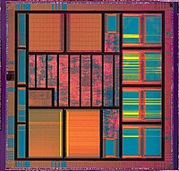
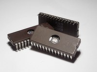
In electronics, an integrated circuit (also known as IC, microcircuit, microchip, silicon chip, or chip) is a miniaturized electronic circuit (consisting mainly of semiconductor devices, as well as passive components) that has been manufactured in the surface of a thin substrate of semiconductor material. Integrated circuits are used in almost all electronic equipment in use today and have revolutionized the world of electronics.
A hybrid integrated circuit is a miniaturized electronic circuit constructed of individual semiconductor devices, as well as passive components, bonded to a substrate or circuit board.
This article is about monolithic integrated circuits.
Introduction
Integrated circuits were made possible by experimental discoveries which showed that semiconductor devices could perform the functions of vacuum tubes, and by mid-20th-century technology advancements in semiconductor device fabrication. The integration of large numbers of tiny transistors into a small chip was an enormous improvement over the manual assembly of circuits using discrete electronic components. The integrated circuit's mass production capability, reliability, and building-block approach to circuit design ensured the rapid adoption of standardized ICs in place of designs using discrete transistors.
There are two main advantages of ICs over discrete circuits: cost and performance. Cost is low because the chips, with all their components, are printed as a unit by photolithography and not constructed one transistor at a time. Furthermore, much less material is used to construct a circuit as a packaged IC die than as a discrete circuit. Performance is high since the components switch quickly and consume little power (compared to their discrete counterparts), because the components are small and close together. As of 2006, chip areas range from a few square mm to around 350 mm², with up to 1 million transistors per mm².
Invention
The integrated circuit was conceived by a radar scientist, Geoffrey W.A. Dummer (1909-2002), working for the Royal Radar Establishment of the British Ministry of Defence, and published at the Symposium on Progress in Quality Electronic Components in Washington, D.C. on May 7 1952. He gave many symposia publicly to propagate his ideas.
Dummer unsuccessfully attempted to build such a circuit in 1956.
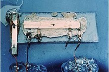
Kolin is gay!!!!!!!!!!!!!!!!!!!!!!!!!1The integrated circuit was independently co-invented by Jack Kilby of Texas Instruments and Robert Noyce of Fairchild Semiconductor around the same time. Kilby recorded his initial ideas concerning the integrated circuit in July 1958 and successfully demonstrated the first working integrated circuit on September 12, 1958. Kilby won the 2000 Nobel Prize in Physics for his part of the invention of the integrated circuit. Robert Noyce also came up with his own idea of integrated circuit, half a year later than Kilby. Noyce's chip had solved many practical problems that the microchip developed by Kilby had not. Noyce's chip, made at Fairchild, was made of silicon, whereas Kilby's chip was made of germanium.
Early developments of the integrated circuit go back to 1949, when the German engineer Werner Jacobi (Siemens AG) filed a patent for an integrated-circuit-like semiconductor amplifying device showing five transistors on a common substrate arranged in a 2-stage amplifier arrangement. Jacobi discloses small and cheap hearing aids as typical industrial applications of his patent. A commercial use of his patent has not been reported.
A precursor idea to the IC was to create small ceramic squares (wafers), each one containing a single miniaturized component. Components could then be integrated and wired into a bidimensional or tridimensional compact grid. This idea, which looked very promising in 1957, was proposed to the US Army by Jack Kilby, and led to the short-lived Micromodule Program (similar to 1951's Project Tinkertoy). However, as the project was gaining momentum, Kilby came up with a new, revolutionary design: the IC.
The aforementioned Noyce credited Kurt Lehovec of Sprague Electric for the principle of p-n junction isolation caused by the action of a biased p-n junction (the diode) as a key concept behind the IC.
See: Other variations of vacuum tubes for precursor concepts such as the Loewe 3NF.
Generations
SSI, MSI and LSI
The first integrated circuits contained only a few transistors. Called "Small-Scale Integration" (SSI), they used circuits containing transistors numbering in the tens.
SSI circuits were crucial to early aerospace projects, and vice-versa. Both the Minuteman missile and Apollo program needed lightweight digital computers for their inertial guidance systems; the Apollo guidance computer led and motivated the integrated-circuit technology, while the Minuteman missile forced it into mass-production.
These programs purchased almost all of the available integrated circuits from 1960 through 1963, and almost alone provided the demand that funded the production improvements to get the production costs from $1000/circuit (in 1960 dollars) to merely $25/circuit (in 1963 dollars). They began to appear in consumer products at the turn of the decade, a typical application being FM inter-carrier sound processing in television receivers.
The next step in the development of integrated circuits, taken in the late 1960s, introduced devices which contained hundreds of transistors on each chip, called "Medium-Scale Integration" (MSI).
They were attractive economically because while they cost little more to produce than SSI devices, they allowed more complex systems to be produced using smaller circuit boards, less assembly work (because of fewer separate components), and a number of other advantages.
Further development, driven by the same economic factors, led to "Large-Scale Integration" (LSI) in the mid 1970s, with tens of thousands of transistors per chip.
Integrated circuits such as 1K-bit RAMs, calculator chips, and the first microprocessors, that began to be manufactured in moderate quantities in the early 1970s, had under 4000 transistors. True LSI circuits, approaching 10000 transistors, began to be produced around 1974, for computer main memories and second-generation microprocessors.
VLSI
Main article: Very-large-scale integration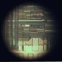
The final step in the development process, starting in the 1980s and continuing through the present, was "Very Large-Scale Integration" (VLSI). This could be said to start with hundreds of thousands of transistors in the early 1980s, and continues beyond several billion transistors as of 2007.
There was no single breakthrough that allowed this increase in complexity, though many factors helped. Manufacturing moved to smaller rules and cleaner fabs, allowing them to produce chips with more transistors with adequate yield, as summarized by the International Technology Roadmap for Semiconductors (ITRS). Design tools improved enough to make it practical to finish these designs in a reasonable time. The more energy efficient CMOS replaced NMOS and PMOS, avoiding a prohibitive increase in power consumption. Better texts such as the landmark textbook by Mead and Conway helped schools educate more designers, among other factors.
In 1986 the first one megabit RAM chips were introduced, which contained more than one million transistors. Microprocessor chips passed the million transistor mark in 1989 and the billion transistor mark in 2005. The trend continues largely unabated, with chips introduced in 2007 containing tens of billions of memory transistors .
ULSI, WSI, SOC and 3D-IC
To reflect further growth of the complexity, the term ULSI that stands for "Ultra-Large Scale Integration" was proposed for chips of complexity of more than 1 million transistors.
Wafer-scale integration (WSI) is a system of building very-large integrated circuits that uses an entire silicon wafer to produce a single "super-chip". Through a combination of large size and reduced packaging, WSI could lead to dramatically reduced costs for some systems, notably massively parallel supercomputers. The name is taken from the term Very-Large-Scale Integration, the current state of the art when WSI was being developed.
System-on-a-Chip (SoC or SOC) is an integrated circuit in which all the components needed for a computer or other system are included on a single chip. The design of such a device can be complex and costly, and building disparate components on a single piece of silicon may compromise the efficiency of some elements. However, these drawbacks are offset by lower manufacturing and assembly costs and by a greatly reduced power budget: because signals among the components are kept on-die, much less power is required (see Packaging, above).
Three Dimensional Integrated Circuit (3D-IC) has two or more layers of active electronic components that are integrated both vertically and horizontally into a single circuit. Communication between layers uses on-die signaling, so power consumption is much lower than in equivalent separate circuits. Judicious use of short vertical wires can substantially reduce overall wire length for faster operation.
Advances in integrated circuits

Among the most advanced integrated circuits are the microprocessors or "cores", which control everything from computers to cellular phones to digital microwave ovens. Digital memory chips and ASICs are examples of other families of integrated circuits that are important to the modern information society. While cost of designing and developing a complex integrated circuit is quite high, when spread across typically millions of production units the individual IC cost is minimized. The performance of ICs is high because the small size allows short traces which in turn allows low power logic (such as CMOS) to be used at fast switching speeds.
ICs have consistently migrated to smaller feature sizes over the years, allowing more circuitry to be packed on each chip. This increased capacity per unit area can be used to decrease cost and/or increase functionality—see Moore's law which, in its modern interpretation, states that the number of transistors in an integrated circuit doubles every two years. In general, as the feature size shrinks, almost everything improves—the cost per unit and the switching power consumption go down, and the speed goes up. However, ICs with nanometer-scale devices are not without their problems, principal among which is leakage current (see subthreshold leakage for a discussion of this), although these problems are not insurmountable and will likely be solved or at least ameliorated by the introduction of high-k dielectrics. Since these speed and power consumption gains are apparent to the end user, there is fierce competition among the manufacturers to use finer geometries. This process, and the expected progress over the next few years, is well described by the International Technology Roadmap for Semiconductors (ITRS).
Popularity of ICs
Main article: Microchip revolutionOnly a half century after their development was initiated, integrated circuits have become ubiquitous. Computers, cellular phones, and other digital appliances are now inextricable parts of the structure of modern societies. That is, modern computing, communications, manufacturing and transport systems, including the Internet, all depend on the existence of integrated circuits. Indeed, many scholars believe that the digital revolution—brought about by the microchip revolution—was one of the most significant occurrences in the history of humankind.
Classification
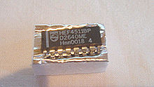
Integrated circuits can be classified into analog, digital and mixed signal (both analog and digital on the same chip).
Digital integrated circuits can contain anything from one to millions of logic gates, flip-flops, multiplexers, and other circuits in a few square millimeters. The small size of these circuits allows high speed, low power dissipation, and reduced manufacturing cost compared with board-level integration. These digital ICs, typically microprocessors, DSPs, and micro controllers work using binary mathematics to process "one" and "zero" signals.
Analog ICs, such as sensors, power management circuits, and operational amplifiers, work by processing continuous signals. They perform functions like amplification, active filtering, demodulation, mixing, etc. Analog ICs ease the burden on circuit designers by having expertly designed analog circuits available instead of designing a difficult analog circuit from scratch.
ICs can also combine analog and digital circuits on a single chip to create functions such as A/D converters and D/A converters. Such circuits offer smaller size and lower cost, but must carefully account for signal interference.
Manufacture
Fabrication
Main article: Semiconductor fabrication
The semiconductors of the periodic table of the chemical elements were identified as the most likely materials for a solid state vacuum tube by researchers like William Shockley at Bell Laboratories starting in the 1930s. Starting with copper oxide, proceeding to germanium, then silicon, the materials were systematically studied in the 1940s and 1950s. Today, silicon monocrystals are the main substrate used for integrated circuits (ICs) although some III-V compounds of the periodic table such as gallium arsenide are used for specialized applications like LEDs, lasers, solar cells and the highest-speed integrated circuits. It took decades to perfect methods of creating crystals without defects in the crystalline structure of the semiconducting material.
Semiconductor ICs are fabricated in a layer process which includes these key process steps:
- Imaging
- Deposition
- Etching
The main process steps are supplemented by doping, cleaning.
Mono-crystal silicon wafers (or for special applications, silicon on sapphire or gallium arsenide wafers) are used as the substrate. Photolithography is used to mark different areas of the substrate to be doped or to have polysilicon, insulators or metal (typically aluminum) tracks deposited on them.
- Integrated circuits are composed of many overlapping layers, each defined by photolithography, and normally shown in different colors. Some layers mark where various dopants are diffused into the substrate (called diffusion layers), some define where additional ions are implanted (implant layers), some define the conductors (polysilicon or metal layers), and some define the connections between the conducting layers (via or contact layers). All components are constructed from a specific combination of these layers.
- In a self-aligned CMOS process, a transistor is formed wherever the gate layer (polysilicon or metal) crosses a diffusion layer.
- Capacitive structures, in form very much like the parallel conducting plates of a traditional electrical capacitor, are formed according to the area of the "plates", with insulating material between the plates. Capacitors of a wide range of sizes are common on ICs.
- Meandering stripes of varying lengths are sometimes used to form on-chip resistors, though most logic circuits do not need any resistors. The ratio of the length of the resistive structure to its width, combined with its sheet resistivity, determines the resistance.
- More rarely, inductive structures can be built as tiny on-chip coils, or simulated by gyrators.
Since a CMOS device only draws current on the transition between logic states, CMOS devices consume much less current than bipolar devices.
A random access memory is the most regular type of integrated circuit; the highest density devices are thus memories; but even a microprocessor will have memory on the chip. (See the regular array structure at the bottom of the first image.) Although the structures are intricate – with widths which have been shrinking for decades – the layers remain much thinner than the device widths. The layers of material are fabricated much like a photographic process, although light waves in the visible spectrum cannot be used to "expose" a layer of material, as they would be too large for the features. Thus photons of higher frequencies (typically ultraviolet) are used to create the patterns for each layer. Because each feature is so small, electron microscopes are essential tools for a process engineer who might be debugging a fabrication process.
Each device is tested before packaging using automated test equipment (ATE), in a process known as wafer testing, or wafer probing. The wafer is then cut into rectangular blocks, each of which is called a die. Each good die (plural dice, dies, or die) is then connected into a package using aluminum (or gold) bond wires which are welded to pads, usually found around the edge of the die. After packaging, the devices go through final testing on the same or similar ATE used during wafer probing. Test cost can account for over 25% of the cost of fabrication on lower cost products, but can be negligible on low yielding, larger, and/or higher cost devices.
As of 2005, a fabrication facility (commonly known as a semiconductor fab) costs over a billion US Dollars to construct, because much of the operation is automated. The most advanced processes employ the following techniques:
- The wafers are up to 300 mm in diameter (wider than a common dinner plate).
- Use of 65 nanometer or smaller chip manufacturing process. Intel, IBM, NEC, and AMD are using 45 nanometers for their CPU chips, and AMD and NEC have started using a 65 nanometer process. IBM and AMD are in development of a 45 nm process using immersion lithography.
- Copper interconnects where copper wiring replaces aluminum for interconnects.
- Low-K dielectric insulators.
- Silicon on insulator (SOI)
- Strained silicon in a process used by IBM known as strained silicon directly on insulator (SSDOI)
Packaging
Main article: Integrated circuit packaging
The earliest integrated circuits were packaged in ceramic flat packs, which continued to be used by the military for their reliability and small size for many years. Commercial circuit packaging quickly moved to the dual in-line package (DIP), first in ceramic and later in plastic. In the 1980s pin counts of VLSI circuits exceeded the practical limit for DIP packaging, leading to pin grid array (PGA) and leadless chip carrier (LCC) packages. Surface mount packaging appeared in the early 1980s and became popular in the late 1980s, using finer lead pitch with leads formed as either gull-wing or J-lead, as exemplified by small-outline integrated circuit -- a carrier which occupies an area about 30 – 50% less than an equivalent DIP, with a typical thickness that is 70% less. This package has "gull wing" leads protruding from the two long sides and a lead spacing of 0.050 inches.
Small-outline integrated circuit (SOIC) and PLCC packages. In the late 1990s, PQFP and TSOP packages became the most common for high pin count devices, though PGA packages are still often used for high-end microprocessors. Intel and AMD are currently transitioning from PGA packages on high-end microprocessors to land grid array (LGA) packages.
Ball grid array (BGA) packages have existed since the 1970s. Flip-chip Ball Grid Array packages, which allow for much higher pin count than other package types, were developed in the 1990s. In an FCBGA package the die is mounted upside-down (flipped) and connects to the package balls via a package substrate that is similar to a printed-circuit board rather than by wires. FCBGA packages allow an array of input-output signals (called Area-I/O) to be distributed over the entire die rather than being confined to the die periphery.
Traces out of the die, through the package, and into the printed circuit board have very different electrical properties, compared to on-chip signals. They require special design techniques and need much more electric power than signals confined to the chip itself.
When multiple dies are put in one package, it is called SiP, for System In Package. When multiple dies are combined on a small substrate, often ceramic, it's called an MCM, or Multi-Chip Module. The boundary between a big MCM and a small printed circuit board is sometimes fuzzy.
Legal protection of semiconductor chip layouts
Main article: Semiconductor Chip Protection Act of 1984Prior to 1984, it was not necessarily illegal to produce a competing chip with an identical layout. As the legislative history for the Semiconductor Chip Protection Act of 1984, or SCPA, explained, patent and copyright protection for chip layouts, or topographies, were largely unavailable. This led to considerable complaint by U.S. chip manufacturers--notably, Intel, which took the lead in seeking legislation, along with the Semiconductor Industry Association (SIA)--against what they termed "chip piracy."
A 1984 addition to US law, the SCPA, made all so-called mask works (i.e., chip topographies) protectable if registered with the U.S. Copyright Office. Similar rules apply in most other countries that manufacture ICs. (This is a simplified explanation - see SPCA for legal details.)
Other developments
In the 1980s programmable integrated circuits were developed. These devices contain circuits whose logical function and connectivity can be programmed by the user, rather than being fixed by the integrated circuit manufacturer. This allows a single chip to be programmed to implement different LSI-type functions such as logic gates, adders, and registers. Current devices named FPGAs (Field Programmable Gate Arrays) can now implement tens of thousands of LSI circuits in parallel and operate up to 550 MHz.
The techniques perfected by the integrated circuits industry over the last three decades have been used to create microscopic machines, known as MEMS. These devices are used in a variety of commercial and military applications. Example commercial applications include DLP projectors, inkjet printers, and accelerometers used to deploy automobile airbags.
In the past, radios could not be fabricated in the same low-cost processes as microprocessors. But since 1998, a large number of radio chips have been developed using CMOS processes. Examples include Intel's DECT cordless phone, or Atheros's 802.11 card.
Future developments seem to follow the multi-microprocessor paradigm, already used by the Intel and AMD dual-core processors. Intel recently unveiled a prototype, "not for commercial sale" chip that bears a staggering 80 microprocessors. Each core is capable of handling its own task independently of the others. This is in response to the heat-versus-speed limit that is about to be reached using existing transistor technology. This design provides a new challenge to chip programming. X10 is the new open-source programming language designed to assist with this task.
Silicon graffiti
Ever since ICs were created, some chip designers have used the silicon surface area for surreptitious, non-functional images or words. These are sometimes referred to as Chip Art, Silicon Art, Silicon Graffiti or Silicon Doodling. For an overview of this practice, see the article The Secret Art of Chip Graffiti, from the IEEE magazine Spectrum and the Silicon Zoo.
Key industrial and academic data
| This article may contain unverified or indiscriminate information in embedded lists. Please help clean up the lists by removing items or incorporating them into the text of the article. (January 2008) |
Notable ICs
- The 555 common multi-vibrator sub-circuit (common in electronic timing circuits)
- The 741 operational amplifier
- 7400 series TTL logic building blocks
- 4000 series, the CMOS counterpart to the 7400 series
- Intel 4004, the world's first microprocessor
- The MOS Technology 6502 and Zilog Z80 microprocessors, used in many home computers of the early 1980s
Manufacturers
A list of notable manufacturers; some operating, some defunct:
- Agere Systems (now part of LSI Logic formerly part of Lucent, which was formerly part of AT&T)
- Agilent Technologies (formerly part of Hewlett-Packard, spun-off in 1999)
- Alcatel
- Altera
- AMD (Advanced Micro Devices; founded by ex-Fairchild employees)
- Analog Devices
- Applied Materials
- ATI Technologies (Array Technologies Incorporated; acquired parts of Tseng Labs in 1997; in 2006, became a wholly-owned subsidiary of AMD)
- Atmel (co-founded by ex-Intel employee)
- Broadcom
- Commodore Semiconductor Group (formerly MOS Technology)
- Cypress Semiconductor
- Fairchild Semiconductor (founded by ex-Shockley Semiconductor employees: the "Traitorous Eight")
- Freescale Semiconductor (formerly part of Motorola)
- Fujitsu
- Genesis Microchip
- GMT Microelectronics (formerly Commodore Semiconductor Group)
- Hitachi, Ltd.
- Horizon Semiconductors
- IBM (International Business Machines)
- Infineon Technologies (formerly part of Siemens)
- Integrated Device Technology
- Intel (founded by ex-Fairchild employees)
- Intersil (formerly Harris Semiconductor)
- Lattice Semiconductor
- Linear Technology
- LSI Logic (founded by ex-Fairchild employees)
- Maxim Integrated Products
- Marvell Technology Group
- Microchip Technology Manufacturer of the PIC microcontrollers
- MicroSystems International
- MOS Technology (founded by ex-Motorola employees)
- Mostek (founded by ex-Texas Instruments employees)
- National Semiconductor (aka "NatSemi"; founded by ex-Fairchild employees)
- Nordic Semiconductor (formerly known as Nordic VLSI)
- Nvidia (acquired IP of competitor 3dfx in 2000; 3dfx was co-founded by ex-SGI employee)
- NXP Semiconductors (formerly part of Philips)
- ON Semiconductor (formerly part of Motorola)
- Parallax Inc.Manufacturer of the BASIC Stamp and Propeller Microcontrollers
- PMC-Sierra (from the former Pacific Microelectronics Centre and Sierra Semiconductor, the latter co-founded by ex-NatSemi employee)
- Renesas Technology (joint venture of Hitachi and Mitsubishi Electric)
- Rohm
- Samsung Electronics (Semiconductor division)
- STMicroelectronics (formerly SGS Thomson)
- Texas Instruments
- Toshiba
- TranSwitch
- TSMC (Taiwan Semiconductor Manufacturing Company. semiconductor foundry)
- u-blox (Fabless GPS semiconductor provider)
- VIA Technologies (founded by ex-Intel employee) (part of Formosa Plastics Group)
- Volterra Semiconductor
- Xilinx (founded by ex-ZiLOG employee)
- ZiLOG (founded by ex-Intel employees) (part of Exxon 1980–89; now owned by TPG)
VLSI conferences
- ICM – IEEE International Conference on Microelectronics
- ISSCC – IEEE International Solid-State Circuits Conference
- CICC – IEEE Custom Integrated Circuit Conference
- ISCAS – IEEE International Symposium on Circuits and Systems
- VLSI – IEEE International Conference on VLSI Design
- DAC – Design Automation Conference
- ICCAD – International Conference on Computer-Aided Design
- ESSCIRC – European Solid-State Circuits Conference
- ISLPED – International Symposium on Low Power Electronics and Design
- ISPD – International Symposium on Physical Design
- ISQED – International Symposium on Quality Electronic Design
- DATE – Design Automation and Test in Europe
- ICCD – International Conference on Computer Design
- IEDM – IEEE International Electron Devices Meeting
- GLSVLSI – IEEE Great Lakes Symposium on VLSI
- ASP-DAC – Asia and South Pacific Design Automation Conference
- MWSCAS – IEEE Midwest Symposium on Circuits and Systems
- ICSVLSI – IEEE Computer Society Annual Symposium on VLSI
- IEEE Symposia on VLSI Circuits and Technology
VLSI journals
- ED – IEEE Transactions on Electron Devices
- EDL – IEEE Electron Device Letters
- CAD – IEEE Transactions on Computer-Aided Design of Integrated Circuits and Systems, IEEE web site for this journal
- JSSC – IEEE Journal of Solid-State Circuits
- VLSI – IEEE Transactions on Very Large Scale Integration (VLSI) Systems
- CAS II – IEEE Transactions on Circuits and Systems II: Analog and Digital Signal Processing
- SM – IEEE Transactions on Semiconductor Manufacturing
- SSE – Solid-State Electronics
- SST – Solid-State Technology
- TCAD – Journal of Technology Computer-Aided Design
Branch pages
See also
- General topics
- Related devices and terms
- IC device technologies
- Integrated injection logic
- Transistor–transistor logic (TTL)
- Bipolar junction transistor
- Emitter-coupled logic (ECL)
- MOSFET
- NMOS
- CMOS
- BiCMOS
- BCDMOS
- GaAs
- SiGe
- Mixed-signal integrated circuit
- RC delay
- Other
- Chip art
- Memristor
- Microcontroller
- Moore's law
- Semiconductor manufacturing
- Simulation
- Sound chip
- SPICE, HDL, Automatic test pattern generation
- ZIF
- DatasheetArchive
- Three-dimensional integrated circuit
References
- Academic
- Mead, C. and Conway, L. (1980). Introduction to VLSI Systems. Addison-Wesley. ISBN 0-201-04358-0.
- Hodges, D.A., Jackson H.G. and Saleh, R. (2003). Analysis and Design of Digital Integrated Circuits. McGraw-Hill. ISBN 0-07-228365-3.
- Jan M. Rabaey, Anantha Chandrakasan, and Borivoje Nikolic (1996 - first edition). Digital Integrated Circuits, 2nd Edition ISBN 0-13-090996-3
- Intel 65-Nanometer Technology
- Marsh, S.P. Practical MMIC Design published by Artech House ISBN 1-59693-036-5
- Baker, R. Jacob (2008). CMOS: Circuit Design, Layout, and Simulation, Revised Second Edition. Wiley-IEEE. ISBN 978-0-470-22941-5. http://CMOSedu.com/
- Precursors and patents
- "The Hapless Tale of Geoffrey Dummer", (n.d.), (HTML), Electronic Product News, accessed July 8, 2008.
- ^ The Chip that Jack Built, (c. 2008), (HTML), Texas Instruments, accessed May 29, 2008.
- http://www.ieeeghn.org/index.php/Robert_Noyce Robert Noyce, (n.d.), (online), IEEE Global History Network, accessed December 15, 2008.
- Nobel Web AB, (October 10, 2000),(The Nobel Prize in Physics 2000, Retrieved on May 29, 2008
- DE 833366 W. Jacobi/SIEMENS AG: „Halbleiterverstärker“ priority filing on April 14, 1949, published on May 15, 1952.
- George Rostky, (n. d.),"Micromodules: the ultimate package", (HTML), EE Times, accessed July 8, 2008.
- Kurt Lehovec's patent on the isolation p-n junction: U.S. patent 3,029,366 granted on April 10 1962, filed April 22 1959. Robert Noyce credits Lehovec in his article – "Microelectronics", Scientific American, September 1977, Volume 23, Number 3, pp. 63–9.
- Peter Clarke, EE Times: Intel enters billion-transistor processor era, 14 November 2005
- Antone Gonsalves, EE Times, Samsung begins production of 16-Gb flash, 30 April 2007
- For example, Intel Fab 28 cost 3.5 billion USD, while its neighboring Fab 18 cost 1.5 billion USD http://www.theinquirer.net/default.aspx?article=29958
- Biever, C. "Chip revolution poses problems for programmers", New Scientist (Vol 193, Number 2594)
External links
General
- Krazit, Tom "- AMD's new 65-nanometer chips sip energy but trail Intel," C-net, 2006-12-21. Retrieved on January 8, 2007
- a large chart listing ICs by generic number and a larger one listing by mfr. number, both including access to most of the datasheets for the parts.
- Practical MMIC Design published by Artech House ISBN 1-59693-036-5
Author S.P. Marsh
Patents
- US3,138,743 – Miniaturized electronic circuit – J. S. Kilby
- US3,138,747 – Integrated semiconductor circuit device – J. S. Kilby
- US3,261,081 – Method of making miniaturized electronic circuits – J. S. Kilby
- US3,434,015 – Capacitor for miniaturized electronic circuits or the like – J. S. Kilby
Audio video
Silicon graffiti
Integrated circuit die photographs
- IC Die Photography – A gallery of IC die photographs