This article has multiple issues. Please help improve it or discuss these issues on the talk page. (Learn how and when to remove these messages)
|
In computing, the clock multiplier (or CPU multiplier or bus/core ratio) sets the ratio of an internal CPU clock rate to the externally supplied clock. This may be implemented with phase-locked loop (PLL) frequency multiplier circuitry. A CPU with a 10x multiplier will thus see 10 internal cycles for every external clock cycle. For example, a system with an external clock of 100 MHz and a 36x clock multiplier will have an internal CPU clock of 3.6 GHz. The external address and data buses of the CPU (often collectively termed front side bus (FSB) in PC contexts) also use the external clock as a fundamental timing base; however, they could also employ a (small) multiple of this base frequency (typically two or four) to transfer data faster.
The internal frequency of microprocessors is usually based on FSB frequency. To calculate internal frequency the CPU multiplies bus frequency by a number called the clock multiplier. For calculation, the CPU uses actual bus frequency, and not effective bus frequency. To determine the actual bus frequency for processors that use dual-data rate (DDR) buses (AMD Athlon and Duron) and quad-data rate buses (all Intel microprocessors starting from Pentium 4) the effective bus speed should be divided by 2 for AMD or 4 for Intel.
Clock multipliers on many modern processors are fixed; it is usually not possible to change them. Some versions of processors have clock multipliers unlocked; that is, they can be "overclocked" by increasing the clock multiplier setting in the motherboard's BIOS setup program. Some CPU engineering samples may also have the clock multiplier unlocked. Many Intel qualification samples have maximum clock multiplier locked: these CPUs may be underclocked (run at lower frequency), but they cannot be overclocked by increasing clock multiplier higher than intended by CPU design. While these qualification samples and majority of production microprocessors cannot be overclocked by increasing their clock multiplier, they still can be overclocked by using a different technique: by increasing FSB frequency.

Basic system structure
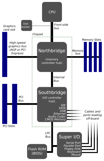
As of 2009, computers have several interconnected devices (CPU, RAM, peripherals, etc. – see diagram) that typically run at different speeds. Thus they use internal buffers and caches when communicating with each other via the shared buses in the system. In PCs, the CPU's external address and data buses connect the CPU to the rest of the system via the "northbridge". Nearly every desktop CPU produced since the introduction of the 486DX2 in 1992 has employed a clock multiplier to run its internal logic at a higher frequency than its external bus, but still remain synchronous with it. This improves the CPU performance by relying on internal cache memories or wide buses (often also capable of more than one transfer per clock cycle) to make up for the frequency difference.
Variants
Some CPUs, such as Athlon 64 and Opteron, handle main memory using a separate and dedicated low-level memory bus. These processors communicate with other devices in the system (including other CPUs) using one or more slightly higher-level HyperTransport links; like the data and address buses in other designs, these links employ the external clock for data transfer timing (typically 800 MHz or 1 GHz, as of 2007).
BIOS settings
Some systems allow owners to change the clock multiplier in the BIOS menu. Increasing the clock multiplier will increase the CPU clock speed without affecting the clock speed of other components. Increasing the external clock (and bus speed) will affect the CPU as well as RAM and other components.
These adjustments provide the two common methods of overclocking and underclocking a computer, perhaps combined with some adjustment of CPU or memory voltages (changing oscillator crystals occurs only rarely); note that careless overclocking can cause damage to a CPU or other component due to overheating or even voltage breakdown. Newer CPUs often have a locked clock multiplier, meaning that the bus speed or the clock multiplier cannot be changed in the BIOS unless the user hacks the CPU to unlock the multiplier. High end CPUs, however, normally have an unlocked clock multiplier.
The earlier motherboards may need to set CPU external frequency and CPU multiplier manually via onboard jumper. Later, in Pentium III and Pentium 4 era, many motherboards can determine CPU frequency automatically via CPUID.
Clock doubling
The phrase clock doubling implies a clock multiplier of two.
Examples of clock-doubled CPUs include:
- the Intel 80486DX2, which ran at 50 or 66 MHz on a 25 or 33 MHz bus
- the Weitek SPARC POWER μP, a clock-doubled 80 MHz version of the SPARC processor that one could drop into the otherwise 40 MHz SPARCStation 2
In both these cases the overall speed of the systems increased by about 75%.
By the late 1990s almost all high-performance processors (excluding typical embedded systems) run at higher speeds than their external buses, so the term "clock doubling" has lost much of its impact.
For CPU-bound applications, clock doubling will theoretically improve the overall performance of the machine substantially, provided the fetching of data from memory does not prove a bottleneck. In more modern processors where the multiplier greatly exceeds two, the bandwidth and latency of specific memory ICs (or the bus or memory controller) typically become a limiting factor.