| This article needs additional citations for verification. Please help improve this article by adding citations to reliable sources. Unsourced material may be challenged and removed. Find sources: "Cyrix Cx486DLC" – news · newspapers · books · scholar · JSTOR (January 2021) (Learn how and when to remove this message) |
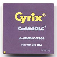
 Cyrix Cx486DLC microprocessor Cyrix Cx486DLC microprocessor | |
| General information | |
|---|---|
| Marketed by | Cyrix, Texas Instruments |
| Designed by | Cyrix |
| Common manufacturer |
|
| Performance | |
| Max. CPU clock rate | 25 MHz to 66 MHz |
| FSB speeds | 25 MHz to 40 MHz |
| Cache | |
| L1 cache | 1 KB (Cx486) 8 KB (TI486SXL) |
| Architecture and classification | |
| Application | Desktop |
| Instruction set | x86-16, IA-32 |
| Physical specifications | |
| Cores |
|
| History | |
| Successor | Cyrix Cx486 |
The Cyrix Cx486DLC is an x86 desktop microprocessor developed by Cyrix. It was Cyrix's second CPU offering, released years after selling math coprocessors that competed with Intel's units and offered better performance at a comparable or lower price. It was released in June of 1992, with a price of $119 for computer manufacturers.
Specifications
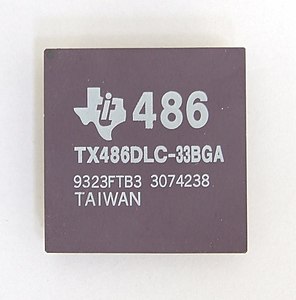
The 486DLC is a 486 desktop CPU from Cyrix, intended to compete with the Intel 486SX and DX. Texas Instruments, who manufactured the 486DLC for Cyrix, later released its own version of the chip, the TI486SXL, with 8 KB internal cache vs 1 KB of the original Cyrix design. The similarly named IBM 486DLC, 486DLC2, 486DLC3 (aka Blue Lightning) are often confused with the Cyrix chips, but are not related and are instead based on Intel's i486 design.
Like the later and more famous Cyrix Cx5x86, it is a hybrid CPU, incorporating features of a new CPU (the Intel 80486) while plugging into its predecessor's (386DX) PGA132 socket. It runs at speeds of 25, 33, and 40 MHz.
The 486DLC can be described as a 386DX with the 486 instruction set and 1 KB of on-board L1 cache added. Because it uses the 386DX bus (unlike its 16-bit cousin, the 486SLC), it is a fully 32-bit chip. Like the 386 and 486SX, it has no on-board math coprocessor, but unlike the 486SX, it can make use of an Intel 387DX or compatible numeric x87 coprocessor. Due to the smaller L1 cache, the 486DLC can not compete on a clock-for-clock basis with the 486SX, but a 33 MHz 486DLC can keep pace with a 25 MHz 486SX, cost less, and offers the ability to upgrade further with the addition of a math coprocessor.
While advertisements from smaller manufacturers touted the superiority of their 486DLC over name-brand computers sporting a 486SX, the only advantage the 486DLC offers over the 486SX is the ability to add a math coprocessor. The Intel 487 "math coprocessor" for 486SX users is a CPU replacement—a 486DX with a different pinout—and originally cost several hundred dollars more than a 387.
As prices on Intel's 486 line fell, Cyrix found it more and more difficult for its 486SLC and DLC CPUs to compete and released a fully pin-compatible version of the 486SX and DX in 1993.
The 486DLC did not see widespread use among large OEMs, but it was widely known among the hardware enthusiast community that an AMD 386DX-40 or Cyrix 486DLC-33 could keep up with a 486SX-25 at a lower cost, so it gained a small following among budget-minded enthusiasts. It was also sometimes used as a replacement for a 386 CPU to give a small speed boost. However, the 486DLC was not designed to be a direct CPU replacement and could lead to stability problems in older boards it was not intended for. "Cyrix-aware" motherboards usually had a few extra cache control lines to maintain cache coherency, as well as CPU register control in the BIOS to enable/disable the on-board cache. Cyrix later released a clock-doubled "direct replacement" upgrade package for 386DX systems called the Cx486DRu2. This kit included a standard 486DLC with an extra "dingus" that sits between the CPU and socket and provides the control lines for cache coherency. These kits were quickly superseded by the Cx486DRx2 CPU, which integrates the cache coherency circuitry into the CPU itself. The Cx486DRx2 appeared on the market in 1994, by which time the 486 was already being displaced by the Pentium. Sales were poor due to the high price and the underwhelming performance compared to a true Intel 486DX2. It was often cheaper to purchase a new 486 motherboard than to invest in an upgrade CPU.
-
Die shot of Cx486DLC
-
 Cyrix Cx486DRx2
-
 Die shot of Cx486DRx2
-
 Cyrix 486DLC, Cyrix 486DRx2, and TI 486DLC/E
-
 TI TX486DLC
Versions
Cx486DLC
TI486DLC
| Model | Bus Speed | Frequency | Cache | Voltage | Notes |
|---|---|---|---|---|---|
| TX486DLC-25-GA | 25 MHz | 25 MHz | 1 KB | 5V | 132-pin PGA package. |
| TX486DLC-33-BGA | 33 MHz | 33 MHz | 1 KB | 5V | |
| TX486DLC/E-33-GA | 33 MHz | 33 MHz | 1 KB | 5V | Advanced power management, 132-pin PGA package. |
| TX486DLC/E-V33-GA | 33 MHz | 33 MHz | 1 KB | 3.3V | Advanced power management, low voltage, 132-pin PGA package. |
| TX486DLC-40-BGA | 40 MHz | 40 MHz | 1 KB | 5V | 132-pin PGA package. |
| TX486DLC/E-40-GA | 40 MHz | 40 MHz | 1 KB | 5V | Advanced power management, 132-pin PGA package. |
TI486SXL
The TI486SXL was Texas Instrument's version of the Cx486DLC. They had 8 KB of cache over the original 1 KB, and a 32-bit bus.
| Model | Bus Speed | Frequency | Cache | Voltage | Notes |
|---|---|---|---|---|---|
| TI486SXL-040S-GA | 20-40 MHz† | 40 MHz | 8 KB | 5V | 132-pin PGA package. |
| TI486SXL2-050S-GA | 25 MHz | 50 MHz | 8 KB | 5V | |
| TI486SXL-040-PCE | 20-40 MHz† | 40 MHz | 8 KB | 5V | 144-pin TEP package. |
| TI486SXL-G40-HBN | 20-40 MHz† | 40 MHz | 8 KB | 3.3, 5V• | 144-pin QFP ceramic package. |
| TI486SXL2-G50-HBN | 25 MHz | 50 MHz | 8 KB | 3.3, 5V• | |
| TI486SXL-040-HBN | 20-40 MHz† | 40 MHz | 8 KB | 5V | |
| TI486SXL2-050-HBN | 25 MHz | 50 MHz | 8 KB | 5V | |
| TI486SXL-G40-GA | 20-40 MHz† | 40 MHz | 8 KB | 3.3, 5V• | 168-pin PGA package. |
| TI486SXL2-G50-GA | 25 MHz | 50 MHz | 8 KB | 3.3, 5V• | |
| TI486SXL2-G66-GA | 33 MHz | 66 MHz | 8 KB | 3.3, 5V• | |
| TI486SXL-V40-GA | 20-40 MHz† | 40 MHz | 8 KB | 3.3V | Low-power version, 168-pin PGA package. |
| TI486SXL2-V50-GA | 25 MHz | 50 MHz | 8 KB | 3.3V | |
| TI486SXL-040-GA | 20-40 MHz† | 40 MHz | 8 KB | 5V | 168-pin PGA package. |
| TI486SXL2-050-GA | 25 MHz | 50 MHz | 8 KB | 5V | |
| † - Can operate at nonclock-doubled 40 MHz or clock-doubled 20/40 MHz.
• - Runs at 3.3V but can tolerate 5V operation. | |||||
Cx486DRx2
| Model | Bus Speed | Frequency | Cache | Voltage | Notes |
|---|---|---|---|---|---|
| Cx486DRx2-25/50 | 25 MHz | 50 MHz | 1 KB | 5V | Upgrade version of the DLC, compatible with 386DX-16, 20, or 25 MHz systems. |
| Cx486DRx2-33/66 | 33 MHz | 66 MHz | 1 KB | 5V | Upgrade version of the DLC, compatible with 386DX-33 MHz systems. |
See also
- Cyrix Cx486SLC - The notebook computer version of the 486DLC.
References
- Quinlan, Tom (8 June 1992). "Cyrix 486DX clone hits Intel hard on price". InfoWorld. Vol. 14, no. 23. InfoWorld Media Group, Inc. p. 17. ISSN 0199-6649. Retrieved 18 February 2022.
- "Cyrix unveils desktop chip". Victoria Advocate. 6 June 1992. Retrieved 21 February 2022.
- "New TI Chips". Computerworld. 11 October 1993. p. 16. Retrieved 21 February 2022.
- "Competition benefits consumers, Advancing technology produces good buys on computer chips". Argus-Leader. 16 April 1993. p. 36. Retrieved 21 February 2022.
- Robert, Lock (October 1995). "Motherboard Buying Guide". Computer. Retrieved 17 October 2018.