| This article needs additional citations for verification. Please help improve this article by adding citations to reliable sources. Unsourced material may be challenged and removed. Find sources: "Decapping" – news · newspapers · books · scholar · JSTOR (November 2020) (Learn how and when to remove this message) |
Decapping (decapsulation) or delidding of an integrated circuit (IC) is the process of removing the protective cover or integrated heat spreader (IHS) of an integrated circuit so that the contained die is revealed for visual inspection of the micro circuitry imprinted on the die. This process is typically done in order to debug a manufacturing problem with the chip, or possibly to copy information from the device, to check for counterfeit chips or to reverse engineer it. Companies such as TechInsights and ChipRebel decap, take die shots of, and reverse engineer chips for customers. Modern integrated circuits can be encapsulated in plastic, ceramic, or epoxy packages.
Delidding may also be done to test the chip for radiation-tolerance with a heavy-ion beam or in an effort to reduce the operating temperatures of an integrated circuit such as a processor, by replacing the thermal interface material (TIM) between the die and the IHS with a higher-quality TIM. With care, it's possible to decap a device and still leave it functional.
Method
Decapping is usually carried out by chemical etching of the covering, laser cutting, laser evaporation of the covering, plasma etching or mechanical removal of the cover using a milling machine, saw blade, using hot air or by desoldering and cutting. The process can be either destructive or non-destructive of the internal die.
Chemical etching usually involves subjecting the (if made of plastic) IC package to concentrated or fuming nitric acid, heated concentrated sulfuric acid, white fuming nitric acid or a mixture of the two for some time, possibly while applying heat externally with a hot plate or hot air gun, which dissolve the package while leaving the die intact. The acids are dangerous, so protective equipment such as appropriate gloves, full face respirator with appropriate acid cartridges, a lab coat and a fume hood are required.
Laser decapping scans a high power laser beam across the plastic IC package to vaporize it, while avoiding the actual silicon die.
In a common version of non-destructive, mechanical delidding, one removes the IHS of an IC such as a computer processor using an oven to soften the solder (if present) between the IHS and the die(s) and using a knife to cut the adhesive in the periphery of the IHS, which joins the IHS with the processor package substrate, which is often a specialized printed circuit board often only called a substrate or sometimes an interposer. In many processors the dies are also soldered to the IHS which can still be removed by applying heat until the solder melts, and removing the IHS while the solder is still liquid. The die(s) are mounted on the substrate using flip chip.
Gallery
-
 AMD Zen 2 EPYC 7702 server processor, before delidding
-
 AMD EPYC 7702 after delidding, with remains of solder thermal interface material (TIM).
-
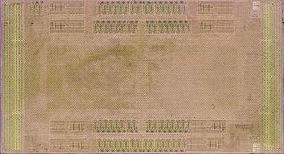
 Removed and flipped over center die before metallization etching; visible are pads for flip chip solder balls
-
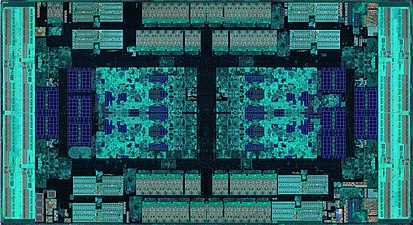
 Die shot of the center die, after removal from processor package substrate and metallization etching.
-
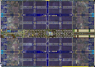
 Die shot of one of the 8 other dies on the processor, after metallization etching.
-
 Copper interconnect (metallization) etching (removal) steps
See also
References
- "MAME devs are cracking open arcade chips to get around DRM – Ars Technica". arstechnica.com. 25 July 2017.
- ^ "How to crack open some computer chips and take your own die shots - ExtremeTech". www.extremetech.com.
- ^ "Don't Try This at Home: Decapping ICs with Boiling Acid".
- Frumusanu, Andrei. "TechInsights Publishes Apple A12 Die Shot: Our Take". www.anandtech.com.
- Frumusanu, Andrei. "ChipRebel Releases Exynos 9820 Die Shot: M4 CPUs in New Cluster". www.anandtech.com.
- "ESA Update on Irradiation Facilities" (PDF). indico.cern.ch.
- "Status of High Energy Irradiation Facilities in Europe" (PDF). nepp.nasa.gov.
- "Electronic Packaging and Space Parts News, EEE Links Vol. 5 No. 2, October 1999" (PDF). ntrs.nasa.gov.
- Fenlon, Wes (26 June 2017). "I performed brain surgery on my CPU to lower its temperature 15 degrees". PC Gamer.
- ^ "Delid and Decap | Semitracks". www.semitracks.com.
- ^ "decap:epoxy [Silicon Pr0n]". siliconpr0n.org.
- alt="">, <img src="//blogger googleusercontent com/img/b/R29vZ2xl/AVvXsEg7E3BNXgac0TBAnhBxBtE1Ha217w0GM_GErwAoTfJYz9mGw7yD0YmkiHrSzr92gADWKnU7NvnnSLgTDnwb6LvsosEDIOxXKD0FL-Wp2RhbMi7CSXjxKi8RP7mLQAuLZlA/s45-c/allisk jpg" width="35" height="35" class="photo". "555 timer teardown: inside the world's most popular IC".
{{cite web}}:|first=has generic name (help)CS1 maint: numeric names: authors list (link) - "Chip Decapping The Easy Way". March 11, 2020.
- ^ "AMD Ryzen Threadripper 3960X Delidded, Tested With Direct-Die Cooling". December 17, 2019.
- "Learn IC Decapping". October 21, 2020.