The gaseous detection device (GDD) is a method and apparatus for the detection of signals in the gaseous environment of an environmental scanning electron microscope (ESEM) and all scanned beam type of instruments that allow a minimum gas pressure for the detector to operate.
History
In the course of development of the ESEM, the detectors previously employed in the vacuum of a scanning electron microscope (SEM) had to be adapted for operation in gaseous conditions. The backscattered electron (BSE) detector was adapted by an appropriate geometry in accordance with the requirements for optimum electron beam transmission, BSE distribution and light guide transmission. However, the corresponding secondary electron (SE) detector (Everhart–Thornley detector) could not be adapted, because the high potential required would cause a catastrophic breakdown even with moderate increase of pressure, such as low vacuum. Danilatos (1983) overcame this problem by using the environmental gas itself as the detector, by virtue of the ionizing action of various signals. With appropriate control of electrode configuration and bias, detection of SE was achieved. A comprehensive survey dealing with the theory and operation of GDD has been published, from which the majority of the material presented below has been used.
Principles and description
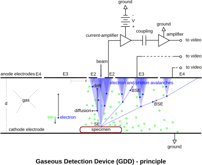
The GDD is in principle an adaptation of techniques for particle detection used in nuclear physics and astronomy. The adaptation involves the parameters required for the formation of images in the conditions of an electron microscope and in the presence of gas inside the specimen chamber. The signals emanating from the beam specimen-interaction, in turn, interact with the surrounding gas in the form of gaseous ionization and excitation. The type, intensity and distribution of signal-gas interactions vary. It is fortunate that generally the time-constant of these interactions is compatible with the time-constant required for the formation of images in the ESEM. The establishment of this compatibility constitutes the basis of the invention of GDD and the leap from particle physics to electron microscopy. The dominant signal-gas interactions are those by the BSE and SE, as they are outlined below.
In its simplest form, the GDD involves one or more electrodes biased with a generally low voltage (e.g. up to 20 V), which is sufficient to collect the ionization current created by whatever sources. This is much the same as an ionization chamber in particle physics. The size and location of these electrodes determine the detection volume in the gas and hence the type of signal detected. The energetic BSE traverse a long distance, whereas the SE travel a much shorter lateral distance mainly by way of diffusion in the gas. Correspondingly, an electrode placed further away from the beam axis will have a predominantly BSE component in comparison to the predominant SE component collected by an electrode placed close to the axis. The precise proportion of signal mix and intensity depends on the additional parameters of gas nature and pressure in conjunction with electrode configurations and bias, bearing in mind that there is no abrupt physical distinction between SE and BSE, apart from the conventional definition of the 50 eV boundary between them.
In another form, the GDD involves one or more electrodes as above but biased with a generally high voltage (e.g. 20–500 V). The processes involved are the same as in the low voltage case with the addition of an amplification of signal along the principle of a proportional amplifier as used in particle physics. That is, all slow electrons in the gas emanating either from the ionizing BSE or directly from the specimen (i.e. the SE) are multiplied in an avalanche form. The energy imparted on the traveling slow electrons by the external electrode field is sufficient to ionize the gas molecules through successive (cascade) collisions. The discharge is controlled in proportion by the applied electrode bias below the breakdown point. This form of detection is referred as ionization-GDD.
Parallel to the ionization, there is also excitation of the gas in both cases above. The gaseous photons are produced both by BSE and SE both directly and by cascade avalanche with the ionization electrons. These photons are detected by appropriate means, like photo-multipliers. By positioning Light tubes strategically, using filters and other light optics means, the SE can again be separated from the BSE and corresponding images formed. This form of detection is referred as scintillation-GDD.
SE distribution and separation

The principles outlined above are best described by considering plane electrodes biased to form a uniform electric field, such as shown in the accompanying diagram of GDD-principle. The electron beam striking the specimen at the cathode effectively creates a point source of SE and BSE. The distribution of slow electrons emitted from a point source inside a gas acted upon by a uniform field is given from the equations (low field):
- with
where R is the fraction of SE that arrives at the anode inside radius r, V the potential difference between the electrodes placed at distance d, k is the Boltzmann constant, T the absolute gas temperature, e the elementary charge and ε is the ratio of the thermal (agitation and kinetic) energy of the electrons divided by the thermal energy of the host gas; I is the corresponding current collected by the anode inside r, δ is the SE yield coefficient and Ib the incident electron beam current. This provides the spatial distribution of the initial electrons SE as they are acted upon by the uniform electric field that moves them from the cathode to the anode, while the electrons also diffuse away due to thermal collisions with the gas molecules. Plots are provided in the accompanying efficiency characteristics of the GDD, for a set of operating conditions of pressure p and distance d. We note that a 100% collection efficiency is fast approached within a small radius even at moderate field strength. At high bias, a nearly complete collection is achieved within a very small radius, a fact that has favorable design implications.
The above radial distribution is valid also in the presence of formation of electron avalanches at high electric field, but it must be multiplied by an appropriate gain factor. In its simplest form for parallel electrodes, the gain factor is the exponential in the current equation:
where α is the first Townsend coefficient. This gives the total signal amplification due to both electrons and ions. The spatial charge distribution and gain factor varies with electrode configuration and geometry and by additional discharge processes described in the referenced theory of the GDD.
BSE distribution
The BSE usually have energies in the kV range so that the much lower electrode bias has only a secondary effect on their trajectory. For the same reason, the finite number of collisions with the gas also results in a second order deflection from their trajectory they would have in vacuum. Therefore, their distribution is practically the same as has been worked out by SEM workers, the variation of which depends on the specimen surface properties (geometry and material composition). For a polished specimen surface the BSE distribution assumes a nearly cosine function but for a rough surface we may take it to be spherical (i.e. uniform in all directions). For brevity, the equations of the second case only are given below. In vacuum, the current distribution from BSE on the electrode is given by
where η is the BSE yield coefficient.
In the presence of gas at low electric field the corresponding equations become:
where S is the ionization coefficient of the gas and p its pressure.
Finally, for a high electric field we get
For practical purposes, the BSE predominantly fall outside the volume acted upon by predominantly the SE, while there is an intermediate volume of comparable fraction of the two signals. The interplay of the various parameters involved has been studied in the main, but it also constitutes a new field for further research and development, especially as we move outside the plane electrode geometry.
Electron and ion induction
Prior to practical implementations, it is helpful to consider a more esoteric aspect (principle), namely, the fundamental physical process taking place in the GDD. The signal in the external circuit is a displacement current i created by induction of charge on the electrodes by a moving charge e with velocity υ in the space between them:
At the point in time when the charge arrives at the electrode, there is no current flowing in the circuit since υ = 0, only when the charge is in motion between the electrodes do we have a signal current. This is important in the case, for example, when a new electron-ion pair is generated at any point in the space between anode-cathode, say at x distance from the anode. Then, only a fraction ex/d of charge is induced by the electron during its transit to the anode, whilst the remainder fraction of e(d − x)/d charge is induced by the ion during its transit to the cathode. Addition of those two fractions gives a charge equal to the charge of one electron. Thus by counting the electrons arriving at the anode or the ions at the cathode we derive the same figure in current measurement. However, since the electrons have a drift velocity about three orders of magnitude greater (in nanosecond range) than the ions, the induced signal may be separated in two components of different significance when the ion transit time may become greater than the pixel time on the scanned image. The GDD has thus two inherent time-constants, a very short one due to the electrons and a longer one due to the ions. When the ion transit time is greater than the pixel dwell time, the useful signal intensity decreases together with an increase of signal background noise or smearing of image edges due to the ions lagging behind. As a consequence, the above derivations, which include the total electron and ion contributions must be modified accordingly with new equations for the case of fast scanning rates. The electrode geometry can be altered with a view to decrease the ion transit time as can be done with a needle or cylindrical geometry.
This fundamental approach helps also understand the so-called “specimen absorbed current” mode of detection in the vacuum SEM, which is limited only to conductive specimens. Image formation of non-conductive specimens now possible in the ESEM, can be understood in terms of an induced displacement current in the external circuit via a capacitor-like action with the specimen being the dielectric between its surface and the underlying electrode. Therefore, the (misnomer) "specimen absorbed current" per se plays no part in any useful image formation except to dissipate the charge (in conductors), without which insulators cannot be generally imaged in vacuum (except in the rare case when the incident beam current equals the total emitted current).
SE detector gain
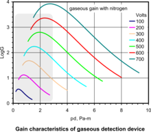
By use of a derivation for the Townsend coefficient given by von Engel, the gain factor G, in the case of SE with total current collection Itot (i.e. for R = 1), is found by:
where A and B are tabulated constants for various gases. In the diagram supplied, we plot the gain characteristics for nitrogen with A = 9.0 and B = 256.5 valid in the range 75–450 V/(Pa·m) for the ratio E/p. We should note that in ESEM work the product pd < 3 Pa·m, since at higher values no useful beam is transmitted through the gas layer to the specimen surface. The gray-shaded area shows the region of GDD operation provided also that the γ processes are very low and do not trigger a breakdown of the proportional amplification. This area contains the maxima of the gain curves, which further re-enforces the successful application of this technology to ESEM. The curves outside the shaded area can be used with beam energy greater than 30 kV, and in future development of environmental or atmospheric transmission scanning electron microscopes employing very high beam energy.
General implementations
The diagram showing the principle of GDD constitutes a versatile implementation that includes not only the SE mode but also the BSE and a combination of these. Even if only the SE signal is desirable to use alone, at least one additional concentric electrode is recommended to employ in order to help in the separation from interference of BSE and also from other noise sources such as the skirt electrons scattered out of the primary beam by the gas. This addition may act as a "guard" electrode, and by varying its bias independently from the SE electrode, the image contrast can be controlled purposefully. Alternative control electrodes are used such as a mesh between anode and cathode. A multipurpose array of electrodes below and above the specimen and above the pressure limiting aperture of the ESEM has also been described elsewhere.
The development of this detector has required devoted electronics circuitry, especially when the signal is picked up by the anode at high bias, because the floating current amplified must be coupled at full bandwidth to the ground amplifier and video display circuits (developed by ElectroScan). An alternative is to bias the cathode with a negative potential and pickup the signal from the anode at floating ground without the need for coupling between amplifier stages. However, this would require extra precaution to protect users from exposure to a high potential at the specimen stage.
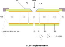
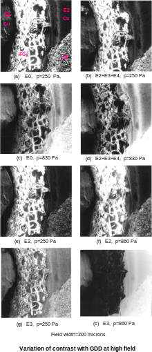
A further alternative that has been implemented at the laboratory stage is by the application of a high bias at the anode but by pickup of the signals from the cathode at floating ground, as shown in the accompanying diagram. Concentric electrodes (E2, E3, E4) are made on a copper-coated fiberglass printed circuit board (PCB) and a copper wire (E1) is added at the center of the disk. The anode is made again from the same PCB with a conical hole (400 micrometres) to act as a pressure limiting aperture in the ESEM. The exposed fiberglass material inside the aperture cone together with its surface above are coated with silver paint in continuity with the copper material of the anode electrode (E0), which is held at high potential. The cathode electrodes are independently connected to ground amplifiers, which, in fact, can be biased with low voltage directly from the amplifier power supplies in the range of ±15 volts without any further coupling required. On account of the induction mechanism operating behind the GDD, this configuration is equivalent to the previous diagram, except for the inverted signal that is electronically restored. While electrode E0 is held at 250 V, meaningful imaging is done as shown by a series of images with composition of signals from various electrodes at two pressures of supplied air. All images show part of the central copper wire (E1), exposed fibreglass (FG, middle), and copper (part of E2) with some silver paint used to attach the wire. The close resemblance of (a) with (b) at low pressure and (c) with (d) at high pressure is a manifestation of the principle of equivalence by induction. The purest SE image is (e) and the purest BSE is (h). Image (f) has prevailing SE characteristics, whilst (g) has a comparable contribution of both SE and BSE. Images (a) and (b) are dominated by SE with some BSE contribution, whilst (c) and (d) have comparable contribution by both SE and BSE.
The very bright areas on the FG material result from genuine high specimen signal yield and not from erratic charging or other artifacts familiar with plastics in vacuum SEM. High yield of edges, oblique incidence, etc. can for the first time be studied from the true surfaces without obstruction in ESEM. Mild charging, if present, may produce stable contrast characteristic of material properties and can be used as a means for studies of the physics of the surfaces. The images presented in this series are reproductions from photographic paper with limited bandwidth, on which attempting to bring up detail in dark areas results in saturating the bright areas and vice versa, whilst a lot more information is usually contained on the negative film. Electronic manipulation of the signal together with modern computer graphics can overcome some old imaging limitations.
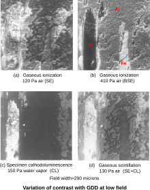
An example of the GDD operating at low voltage is shown with four images of the same field of view of a polished mineral containing aluminum, iron, silicon and some unknown surface impurities. The anode electrode is a single thin wire placed on the side and below the specimen surface, several mm away from it. Image (a) shows predominantly SE contrast at low pressure, whilst (b) shows BSE material contrast at higher pressure. Image (c) shows cathodoluminescence (CL) from the specimen surface by use of water vapor (which does not scintillate), whilst (d) shows additional photon signal by changing the gas to air which scintillates by signal electrons originating from the specimen. The latter appears to be a mixture of CL with SE, but it may also contain additional information from the surface contaminant charging to a varying degree with gas pressure.
The GDD at high voltage has clear advantages over the low voltage mode, but the latter may be used easily with special applications such as at very high pressures where the BSE produce a high ionization gain from their own high energy, or in cases when the electric field requires shaping to purposeful ends. In general, the detector should be designed to operate at both high and low bias levels including variable negative (electron retarding) bias with important contrast generation.
Further improvements have been envisaged, such as the use of special electrode materials, gas composition and shaping the trajectory of detection electrons by special electric and magnetic fields (page 91).
Further developments
The above described principles have been further implemented in ESEM with detection of secondary and backscattered electrons for 3D imaging with multi-detector method by Slowko et al. Fitzek et al. have rectified some drawbacks of an available commercial ESEM by optimizing the pressure limiting system and the secondary electron detection resulting in high-quality imaging.
Commercial implementations
The first commercial implementation of the GDD was carried out by ElectroScan Corporation employing the acronym ESD for "environmental secondary detector", which was followed by an improved version termed "gaseous secondary electron detector" (GSED). The use of the magnetic field of the objective lens of the microscope has been incorporated in another commercial patent. LEO company (now Carl Zeiss SMT) has used the scintillation mode and the ionization (needle) mode of the GDD on its environmental SEMs at low and also extended pressure range.
References
- Danilatos, G.D. (1985). "Design and construction of an atmospheric or environmental SEM (part 3)". Scanning. 7: 26–42. doi:10.1002/sca.4950070102.
- Danilatos, G.D. (1983a) Gaseous detector device for an environmental electron probe microanalyzer. Research Disclosure No. 23311:284.
- Danilatos, G.D. (1983). "A gaseous detector device for an environmental SEM". Micron and Microscopica Acta. 14 (4): 307–318. doi:10.1016/0047-7206(83)90002-X.
- ^ Danilatos, G.D. (1990) Theory of the Gaseous Detector Device in the ESEM. Advances in Electronics and Electron Physics, Academic Press, Vol. 78:1–102.
- Huxley AG, Zaazou AA (1949). "Experimental and theoretical studies of slow electrons in air". Proceedings of the Royal Society. 196 (1046): 402–426. Bibcode:1949RSPSA.196..402H. doi:10.1098/rspa.1949.0035. PMID 18127588.
- ^ A von Engel (1965) book "Ionised Gases" Oxford at the Clarendon Press
- ^ Danilatos, G.D. (1990). "Equations of charge distribution in the ESEM". Scanning Microscopy. 4 (4): 799–823.
- Danilatos GD (2009). "Optimum beam transfer in the ESEM". J. Microsc. 234 (1): 26–37. doi:10.1111/j.1365-2818.2009.03148.x. PMID 19335454. S2CID 33207923.
- ^ U.S. patent 4,897,545, filed October 14, 1988 (priority date October 16, 1987, Australia PI4918). Assigned to ElectroScan Corp. Inventor: GD Danilatos
- ^ Danilatos, G.D. (1990). "Mechanisms of detection and imaging in the ESEM". J. Microsc. 160: 9–19. doi:10.1111/j.1365-2818.1990.tb03043.x. S2CID 97707382.
- Danilatos, G.D. (1986). "Cathodoluminescence and gaseous scintillation in the environmental SEM". Scanning. 8 (6): 279–284. doi:10.1002/sca.4950080605.
- Slowko, W. (2018). "Detection of secondary and backscattered electrons for 3D imaging with multi-detector method in VP/ESEM". Micron. 104: 45–60. doi:10.1016/j.micron.2017.10.002. PMID 29080547.
- Fitzek, H.; Schroetner, H.; Wagner, J.; Hofer, F. & Rattenberger, J. (2016). "High-quality imaging in environmental scanning electron microscopy - optimizing the pressure limiting system and the secondary electron detection of a commercially available ESEM". Journal of Microscopy. 216 (1): 185–91. doi:10.1111/jmi.12347. PMID 26540292. S2CID 206085524.
{{cite journal}}: CS1 maint: multiple names: authors list (link) - U.S. patent 4,785,182, filed May 21, 1987. Secondary electron detector for use in a gaseous atmosphere. Inventors: J.F. Mancuso, W.B. Maxwell, G.D. Danilatos. Assignee: ElectroScan Corporation.
- U.S. patent 6,972,412, (December 6, 2005) Particle-optical device and detection means. Inventors: Scholtz Jacob Johannes, Knowles W. Ralph, Thiel Bradley Lamar, Van Veen Gerardus, Schroemges Rene Peter Marie
- "Carl Zeiss SMT ESEM". Archived from the original on 2009-04-17. Retrieved 2009-07-01.
 with
with 


