| This article needs additional citations for verification. Please help improve this article by adding citations to reliable sources. Unsourced material may be challenged and removed. Find sources: "GDDR3 SDRAM" – news · newspapers · books · scholar · JSTOR (December 2006) (Learn how and when to remove this message) |
| Type of RAM | |
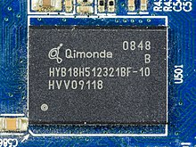
 GDDR3 chips on a AMD Radeon HD 4670 GDDR3 chips on a AMD Radeon HD 4670 | |
| Developer | JEDEC |
|---|---|
| Type | Synchronous dynamic random-access memory |
| Generation | 3rd generation |
| Predecessor | GDDR2 SDRAM |
| Successor | GDDR4 SDRAM |


GDDR3 SDRAM (Graphics Double Data Rate 3 SDRAM) is a type of DDR SDRAM specialized for graphics processing units (GPUs) offering less access latency and greater device bandwidths. Its specification was developed by ATI Technologies in collaboration with DRAM vendors including Elpida Memory, Hynix Semiconductor, Infineon (later Qimonda) and Micron. It was later adopted as a JEDEC standard.
Overview
It has much the same technological base as DDR2, but the power and heat dispersal requirements have been reduced somewhat, allowing for higher performance memory modules, and simplified cooling systems. GDDR3 is not related to the JEDEC DDR3 specification. This memory uses internal terminators, enabling it to better handle certain graphics demands. To improve throughput, GDDR3 memory transfers 4 bits of data per pin in 2 clock cycles.
The GDDR3 interface transfers two 32 bit wide data words per clock cycle from the I/O pins. Corresponding to the 4n-prefetch a single write or read access consists of a 128 bit wide, one-clock-cycle data transfer at the internal memory core and four corresponding 32 bit wide, one-half-clock-cycle data transfers at the I/O Pins. Single-ended unidirectional Read and Write Data strobes are transmitted simultaneously with Read and Write data respectively in order to capture data properly at the receivers of both the Graphics SDRAM and the controller. Data strobes are organized per byte of the 32 bit wide interface.
Commercial implementation
Despite being designed by ATI, the first card to use the technology was nVidia's GeForce FX 5700 Ultra in early 2004, where it replaced the GDDR2 chips used up to that time. The next card to use GDDR3 was nVidia's GeForce 6800 Ultra, where it was key in maintaining reasonable power requirements compared to the card's predecessor, the GeForce 5950 Ultra. ATI began using the memory on its Radeon X800 cards. GDDR3 was Sony's choice for the PlayStation 3 gaming console's graphics memory, although its nVidia based GPU is also capable of accessing the main system memory, which consists of XDR DRAM designed by Rambus Incorporated (Similar technology is marketed by nVidia as TurboCache in PC platform GPUs). Microsoft's Xbox 360 has 512 MB of GDDR3 memory. Nintendo's Wii also contains 64 MB of GDDR3 memory.
Advantages of GDDR3 over DDR2
- GDDR3's strobe signal unlike DDR2 SDRAM is unidirectional & single-ended (RDQS, WDQS). This means there is a separate read and write data strobe allowing for a quicker read to write ratio than DDR2.
- GDDR3 has a hardware reset capability allowing it to flush all data from memory and then start again.
- Lower voltage requirements leads to lower power requirements, and lower heat output.
- Higher clock frequencies, due to lower heat output, this is beneficial for increased throughput and more precise timings.
See also
References
- "ATI Technologies Promotes GDDR3". Archived from the original on 2002-12-07. Retrieved 2002-12-07.
- Gregory Agostinelli. "Method and Apparatus for fine tuning a memory interface". US PATENT OFFICE.
External links
| Dynamic random-access memory (DRAM) | |
|---|---|
| Asynchronous | |
| Synchronous | |
| Graphics | |
| Rambus | |
| Memory modules | |
| Lists | |
| Graphics processing unit | |||||
|---|---|---|---|---|---|
| GPU |
| ||||
| Architecture | |||||
| Components | |||||
| Memory | |||||
| Form factor | |||||
| Performance | |||||
| Misc | |||||