| This article includes a list of general references, but it lacks sufficient corresponding inline citations. Please help to improve this article by introducing more precise citations. (October 2019) (Learn how and when to remove this message) |

The MC88110 was a microprocessor developed by Motorola that implemented the 88000 instruction set architecture (ISA). The MC88110 was a second-generation implementation of the 88000 ISA, succeeding the MC88100. It was designed for use in personal computers and workstations.
History
The first technical description of the MC88110 was given in November 1991 at the Microprocessor Forum held in San Francisco. The microprocessor was introduced in 1992, operating at 50 MHz. Users were Data General in their AViiON servers, Harris in real-time UNIX systems and Motorola in their single-board computers. NeXT was to introduce a workstation using the MC88110, the NeXT RISC Workstation, but they left the hardware business and cancelled the product before development had completed.
Description

It implemented extensions to the original ISA, such a separate floating-point register file, extended-precision (80-bit) floating-point data types and new integer and graphics instructions. It also implemented microarchitectural features previously non-existent in 88000 microprocessors, such as two-way superscalar execution, out-of-order completion and speculative execution. Despite these new features, which corrected some architectural deficiencies in the MC88100, the MC88110 was ultimately unsuccessful and was used in few systems. The MC88110 was succeeded by PowerPC microprocessors Motorola developed jointly with IBM as part of the AIM alliance, but remained available until the mid-1990s.
Externally the 88110 has a von Neumann architecture (single memory for code and data) with a modified Harvard architecture internally (separate instruction and data caches).
The MC88110 supported an optional external 256 KB to 2 MB secondary cache. The secondary cache controller was not integrated on the MC88110, but was located on a separate device, the MC88410, to reduce cost.
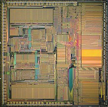
The die contained 1.3 million transistors and measured 15 mm by 15 mm (225 mm). It was fabricated in a 1 μm complementary metal–oxide–semiconductor (CMOS) process. The process has three levels of aluminium interconnect and an effective channel length (the distance between the source and drain contacts of the MOSFET transistors) of 0.8 μm. The MC88110 was designed to be shrunk to a 0.8 μm process with an effective channel length of 0.65 μm without modification.
Notes
- This differs from its predecessor, the 88100, which had a Harvard architecture and required the addition of a pair of 88200 chips to instead use a unified memory.
References
- MC88110 User's Manual, Figure 1-3.
- MC88100 User's Manual, Figure 1-2 and §1.2.7.
- Diefendorff, Keith; Allen, Michael (April 1992). "Organization of the Motorola 88110 Superscalar RISC Microprocessor". IEEE Micro. 12 (2): 40–63. doi:10.1109/40.127582. S2CID 25668727.
- Tabak, Daniel (1995). Advance Microprocessors (2 ed.). McGraw-Hill. pp. 425–435.
- Motorola, Inc., ed. (1991). MC88110 Second Generation RISC Microprocessor User's Manual (PDF). Motorola databook series. OCLC 29333909. Retrieved 25 August 2023.
- Motorola, Inc., ed. (1990). MC88100 RISC Microprocessor User's Manual (PDF) (2nd ed.). Prentice Hall. ISBN 013567090X. Retrieved 25 August 2023.
| Motorola-Freescale-NXP processors and microcontrollers | |||||||||||||||||||||
|---|---|---|---|---|---|---|---|---|---|---|---|---|---|---|---|---|---|---|---|---|---|
| |||||||||||||||||||||
| |||||||||||||||||||||