| This article includes a list of references, related reading, or external links, but its sources remain unclear because it lacks inline citations. Please help improve this article by introducing more precise citations. (November 2017) (Learn how and when to remove this message) |
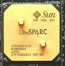
 A 200 MHz UltraSPARC microprocessor A 200 MHz UltraSPARC microprocessor | |
| General information | |
|---|---|
| Launched | 1995 |
| Discontinued | 1997 |
| Designed by | Sun Microsystems |
| Performance | |
| Max. CPU clock rate | 143 MHz to 200 MHz |
| Architecture and classification | |
| Instruction set | SPARC V9 |
| Physical specifications | |
| Cores |
|
| History | |
| Predecessor | SuperSPARC II |
| Successor | UltraSPARC II |
The UltraSPARC is a microprocessor developed by Sun Microsystems and fabricated by Texas Instruments, introduced in mid-1995. It is the first microprocessor from Sun to implement the 64-bit SPARC V9 instruction set architecture (ISA). Marc Tremblay was a co-microarchitect.
Microarchitecture
The UltraSPARC is a four-issue superscalar microprocessor that executes instructions in in-order. It includes a nine-stage integer pipeline.
Functional units
The execution units were simplified relative to the SuperSPARC to achieve higher clock frequencies - an example of a simplification is that the ALUs were not cascaded, unlike the SuperSPARC, to avoid restricting clock frequency.
The integer register file has 32 64-bit entries. As the SPARC ISA uses register windows, of which the UltraSPARC has eight, the actual number of registers is 144. The register file has seven read and three write ports. The integer register file provides registers to two arithmetic logic units and the load/store unit. The two ALUs can both execute arithmetic, logic and shift instructions but only one can execute multiply and divide instructions.
The floating-point unit consists of five functional units. One executes floating point adds and subtracts, one multiplies, one divides and square-roots. Two units are for executing SIMD instructions defined by the Visual Instruction Set (VIS). The floating-point register file contains thirty-two 64-bit registers. It has five read ports and three write ports.
Cache
The UltraSPARC has two levels of cache, primary and secondary. There are two primary caches, one for instructions and one for data. Both have a capacity of 16 KB.
The UltraSPARC required a mandatory external secondary cache. The cache is unified, has a capacity of 512 KB to 4 MB and is direct-mapped. It can return data in a single cycle. The external cache is implemented with synchronous SRAMs clocked at the same frequency as the microprocessor, as ratios were not supported. It is accessed via the data bus.
Fabrication
It contained 3.8 million transistors. It was fabricated in Texas Instruments' EPIC-3 process, a 0.5 μm complementary metal–oxide–semiconductor (CMOS) process with four levels of metal. The UltraSPARC was not fabricated in a BiCMOS process as Texas Instruments claimed it did not scale well to 0.5 μm processes and offered little performance improvement. The process was perfected on TI's MVP digital signal processor (DSP) with some features missing such as three levels of metal instead of four and a 0.55 feature size, before it was used to fabricate the UltraSPARC to avoid a repeat of the fabrication problems encountered with SuperSPARC.
Package
The UltraSPARC is packaged in a 521-contact plastic ball grid array (PBGA).
Related processors
References
- Greenley, D. et al. (1995). "UltraSPARC: The next generation superscalar 64-bit SPARC". Proceedings of Compcon '95: pp. 442–451.
- Gwennap, Linley (3 October 1994). "UltraSparc Unleashes SPARC Performance". Microprocessor Report, Volume 8, Number 13.
- Gwennap, Linley (5 December 1994). "UltraSparc Adds Multimedia Instructions". Microprocessor Report.
| Sun Microsystems | ||||||||
|---|---|---|---|---|---|---|---|---|
| Acquired by Oracle | ||||||||
| Hardware |
| |||||||
| Software | ||||||||
| Storage | ||||||||
| Performance | ||||||||
| Research | ||||||||
| Education | ||||||||
| Community |
| |||||||
| Acquisitions | ||||||||
| Slogans | ||||||||
| Category | ||||||||