| This article needs to be updated. The reason given is: Needs updated introduction and newer products. Please help update this article to reflect recent events or newly available information. (December 2024) |
 Latest logo used from 2020 to 2023 Latest logo used from 2020 to 2023 | |
| General information | |
|---|---|
| Launched | April 15, 1998; 26 years ago (1998-04-15) |
| Discontinued | 2023; 1 year ago (2023) |
| Marketed by | Intel |
| Designed by | Intel |
| Common manufacturer | |
| Performance | |
| Max. CPU clock rate | 266 MHz to 3.6 GHz |
| FSB speeds | 66 MHz to 1333 MT/s |
| DMI speeds | 2.0 GT/s to 16 GT/s |
| Architecture and classification | |
| Technology node | 250 nm to Intel 7 (10ESF) |
| Microarchitecture | |
| Instruction set | IA-32, x86-64 |
| Instructions | x86 |
| Physical specifications | |
| Cores |
|
| Sockets | |
| Products, models, variants | |
| Core names |
|
| Variant | |
| History | |
| Predecessors | i486, Pentium II |
| Successor | Intel Processor |
Celeron is a series of IA-32 and x86-64 computer microprocessors targeted at low-cost personal computers, manufactured by Intel from 1998 until 2023.
The first Celeron-branded CPU was introduced on April 15, 1998, and was based on the Pentium II. Celeron-branded processors released from 2009 to 2023 are compatible with IA-32 software. They typically offer less performance per clock speed compared to flagship Intel CPU lines, such as the Pentium or Core brands. They often have less cache or intentionally disabled advanced features, with variable impact on performance. While some Celeron designs have achieved strong performance for their segment, the majority of the Celeron line has exhibited noticeably degraded performance. This has been the primary justification for the higher cost of other Intel CPU brands versus the Celeron range.
In September 2022, Intel announced that the Celeron brand, along with Pentium, were to be replaced with the new "Intel Processor" branding for low-end processors in laptops from 2023 onwards. This applied to desktops using Celeron processors as well, and was discontinued around the same time laptops stopped using Celeron processors in favor of "Intel Processor" processors in 2023.
Background
As a product concept, the Celeron was introduced in response to Intel's loss of the low-end market, in particular to the Cyrix 6x86, the AMD K6, and the IDT Winchip. Intel's existing low-end product, the Pentium MMX, was no longer performance-competitive at 233 MHz. Although a faster Pentium MMX would have been a lower-risk strategy, the industry-standard Socket 7 platform hosted a market of competitor CPUs that could be drop-in replacements for the Pentium MMX. Instead, Intel pursued a budget part that was to be pin-compatible with their high-end Pentium II product, using the Pentium II's proprietary Slot 1 interface.
The Celeron also effectively killed off the nine-year-old 80486 chip, which had been the low-end processor brand for entry-level desktops and laptops until 1998.
Intel hired marketing firm Lexicon Branding, which had originally come up with the name "Pentium", to devise a name for the new product as well. The San Jose Mercury News described Lexicon's reasoning behind the name they chose: "Celer is Latin for swift, as in the word 'accelerate', and 'on' as in 'turned on'. Celeron is seven letters and three syllables, like Pentium. The 'Cel' of Celeron rhymes with 'tel' of Intel."
| Based on | Desktop | Laptop | Embedded | ||||||
|---|---|---|---|---|---|---|---|---|---|
| Code-named | Core | Date released | Code-named | Core | Date released | Code-named | Core | Date released | |
| P6 | Covington Mendocino Coppermine-128 Tualatin-256 |
(250 nm) (250 nm) (180 nm) (130 nm) |
1998 1998–2000 2000–2001 2002 |
Mendocino Coppermine-128 Coppermine T |
(250 nm) (180 nm) (180 nm) |
1999 2000–2001 2001 |
|||
| NetBurst | Willamette-128 Northwood-128 |
(180 nm) (130 nm) |
2002 2002–2003 |
Northwood-256 |
(130 nm) |
2002–2003 | |||
| Pentium M (Celeron M) | Banias-512 Dothan-512 Dothan-1024 Yonah-512 Yonah-1024 |
(130 nm)
(90 nm) (90 nm) (65 nm) |
2004
2004–2007 2004–2005 2007 2006 2006–2007 | ||||||
| NetBurst (Celeron D) | Prescott-256 Cedar Mill-512 |
(90 nm) (65 nm) |
2004–2005 2006–2007 |
||||||
| Core (Single) | Conroe-L
Conroe-CL |
(65 nm)
(65 nm) |
2007-2008
??? | ||||||
| Core (Dual) | Allendale Wolfdale-3M |
(65 nm) (45 nm) |
2008–2009
2009–2010 | ||||||
| Core (Celeron M/Celeron) | Merom, Merom-L
Merom-2M Merom-L (Ultra-Low-Voltage) |
(65 nm) (65 nm) (65 nm) |
2007–2008
2008 2007, 2009 | ||||||
| Core (Celeron Dual) | Merom-2M
Penryn-3M |
(65 nm)
(45 nm) |
2008
2009–2010 | ||||||
| Nehalem/Westmere | Clarkdale | (32 nm) | 2010 | Arrandale | (32 nm) | 2010–2011 | |||
| Jasper Forest | Single (45 nm) | ||||||||
| Silvermont
Airmont Goldmont Goldmont Plus Tremont |
Bay Trail-
Braswell Apollo Lake Gemini Lake Jasper Lake |
dual & quad (22 nm)
dual & quad (14 nm) up to quad (14 nm) up to quad (14 nm) up to quad (10 nm) |
Bay Trail-M
Braswell Apollo Lake Gemini Lake Jasper Lake |
dual & quad (22 nm)
dual & quad (14 nm) up to quad (14 nm) up to quad (14 nm) up to quad (10 nm) |
October 2013
March 2015 April 2016 December 2017 January 2021 |
Bay Trail-M
Braswell Apollo Lake Gemini Lake Jasper Lake |
dual & quad (22 nm)
dual & quad (14 nm) up to quad (14 nm) up to dual (14 nm) up to dual (10 nm) |
October 2013
March 2015 April 2016 December 2017 January 2021 | |
| List of Intel Celeron processors | |||||||||
Desktop Celerons
P6-based Celerons
Main article: List of Intel Celeron microprocessors § P6 based CeleronsCovington

Launched in April 1998, the first Covington Celeron was essentially a 266 MHz Pentium II manufactured without any secondary cache at all. Covington also shared the 80523 product code of Deschutes. Although clocked at 266 or 300 MHz (frequencies 33 or 66 MHz higher than the desktop version of the Pentium w/MMX), the cacheless Celerons had trouble outcompeting the parts they were designed to replace. Substantial numbers were sold on first release, largely on the strength of the Intel name, but the Celeron quickly achieved a poor reputation both in the trade press and among computer professionals. The initial market interest faded rapidly in the face of its poor performance, and with sales at a very low level, Intel felt obliged to develop a substantially faster replacement as soon as possible. Nevertheless, the first Celerons were quite popular among some overclockers, for their flexible overclockability and reasonable price. Covington was only manufactured in Slot 1 SEPP format.
Mendocino


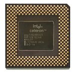

The Mendocino Celeron, launched August 24, 1998, was the first retail CPU to use on-die L2 cache. Whereas Covington had no secondary cache at all, Mendocino included 128 KB of L2 cache running at full clock rate. The first Mendocino-core Celeron was clocked at a then-modest 300 MHz but offered almost twice the performance of the old cacheless Covington Celeron at the same clock rate. To distinguish it from the older Covington 300 MHz, Intel called the Mendocino core Celeron 300A. Although the other Mendocino Celerons (the 333 MHz part, for example) did not have an A appended, some people call all Mendocino processors Celeron-A regardless of clock rate.
The new Mendocino-core Celeron was a good performer from the outset. Indeed, most industry analysts regarded the first Mendocino-based Celerons as too successful—performance was sufficiently high to not only compete strongly with rival parts, but also to attract buyers away from Intel's high-profit flagship, the Pentium II. Overclockers soon discovered that, given a high-end motherboard, many Celeron 300A CPUs could run reliably at 450 MHz. This was achieved by simply increasing the front-side bus (FSB) clock rate from the stock 66 MHz to the 100 MHz clock of the Pentium II, helped by several facts: the 440BX chipset with nominal support for 100 MHz and correspondent memory had already been on the market, and the internal L2 cache was more tolerant to overclocking than external cache chips, which already had to run at half-CPU speed by design. At this frequency, the budget Mendocino Celeron rivaled the fastest x86 processors available. Some motherboards were designed to prevent this modification, by restricting the Celeron's front side bus to 66 MHz. However, overclockers soon found that putting tape over pin B21 of the Celeron's interface slot circumvented this, allowing a 100 MHz bus.
At the time on-die cache was difficult to manufacture; especially L2 as more of it is needed to attain an adequate level of performance. A benefit of on-die cache is that it operates at the same clock rate as the CPU. All other Intel CPUs at that time used motherboard mounted or slot mounted secondary L2 cache, which was very easy to manufacture, cheap, and simple to enlarge to any desired size (typical cache sizes were 512 KB or 1 MB), but they carried the performance penalty of slower cache performance, typically running at a FSB frequency of 60 to 100 MHz. The Pentium II's 512 KB of L2 cache was implemented with a pair of relatively high-performance L2 cache chips mounted on a special-purpose board alongside the processor itself, running at half the processor's clock rate and communicating with the CPU through a special back-side bus. This method of cache placement was expensive and imposed practical cache-size limits, but allowed the Pentium II to be clocked higher and avoided front side bus RAM/L2 cache contention typical with motherboard-placed L2 cache configurations.
Over time, newer Mendocino processors were released at 333, 366, 400, 433, 466, 500, and 533 MHz. The Mendocino Celeron CPU came only designed for a 66 MHz front-side bus, but this would not be a serious performance bottleneck until clock rates reached higher levels.
The Mendocino Celerons also introduced new packaging. When the Mendocinos debuted they came in both a Slot 1 SEPP and Socket 370 PPGA package. The Slot 1 form had been designed to accommodate the off-chip cache of the Pentium II and had mounting problems with motherboards. Because all Celerons are a single-chip design, however, there was no reason to retain the slot packaging for L2 cache storage, and Intel discontinued the Slot 1 variant; beginning with the 466 MHz part, only the PPGA Socket 370 form was offered. (Third-party manufacturers made motherboard slot-to-socket adapters (nicknamed Slotkets) available for a few dollars, which allowed, for example, a Celeron 500 to be fitted to a Slot 1 motherboard.) One interesting note about the PPGA Socket 370 Mendocinos is they supported symmetric multiprocessing (SMP), and there was at least one motherboard released (the ABIT BP6) which took advantage of this fact.
The Mendocino also came in a mobile variant, with clock rates of 266, 300, 333, 366, 400, 433 and 466 MHz.
In Intel's "Family/Model/Stepping" scheme, Mendocino CPUs are family 6, model 6 and their Intel product code is 80524. These identifiers are shared with the related Dixon Mobile Pentium II variant.
Coppermine-128
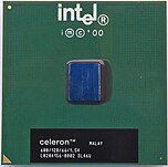 Celeron Coppermine 128 600 MHz (FC-PGA package)
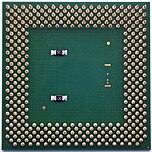 Underside of a Celeron Coppermine 128, 600 MHz
The next generation Celeron was the 'Coppermine-128' (sometimes known as the Celeron II). These were a derivative of Intel's Coppermine Pentium III and were released on March 29, 2000. This Celeron used a Coppermine core with half of its L2 cache switched off, resulting in 128 KB of 4-way associative on-chip L2 cache as on the Mendocino, and was initially likewise restricted to a 66 MHz Front Side Bus speed. Despite the halved associativity on the L2 cache, which reduced hit rates compared to the full Coppermine design, it kept the 256-bit wide L2 cache bus, which meant an advantage compared to Mendocino and older Katmai/Pentium II designs, which all had a 64-bit datapath to their L2 caches. SSE instructions were also enabled.
All Coppermine-128s were produced in the same FCPGA Socket 370 format that most Coppermine Pentium III CPUs used. These Celeron processors began at 533 MHz and continued through 566, 600, 633, 667, 700, 733, and 766 MHz. Because of the limitations of the 66 MHz bus, there were diminishing returns on performance as clock rates increased. On January 3, 2001, Intel switched to a 100 MHz bus with the launch of the 800 MHz Celeron, resulting in a significant performance-per-clock improvement. All Coppermine-128 CPUs from 800 MHz and higher use the 100 MHz front side bus. Various models were made at 800, 850, 900, 950, 1000, and 1100 MHz.
In Intel's "Family/Model/Stepping" scheme, Coppermine Celerons and Pentium IIIs are family 6, model 8 and their Intel product code is 80526.
Tualatin-256

These Celeron processors, released initially at 1.2 GHz on October 2, 2001, were based on the Pentium III 'Tualatin' core and made with a 0.13 micrometer process for the FCPGA 2 Socket 370. They were nicknamed "Tualeron" by some enthusiasts — a portmanteau of the words Tualatin and Celeron. Some software and users refer to the chips as Celeron-S, referring to the chip's lineage with the Pentium III-S, but this is not an official designation. Intel later released 1 GHz and 1.1 GHz parts (which were given the extension A to their name to differentiate them from the Coppermine-128 of the same clock rate they replaced). A 1.3 GHz chip, launched January 4, 2002, and finally a 1.4 GHz chip, launched May 15, 2002 (the same day as the 1.7 GHz Willamette-based Celeron launch), marked the end of the Tualatin-256 line.
The most significant differences compared to the Pentium III Tualatin are a lower 100 MHz bus and fixed 256 KB of L2 cache (whereas the Pentium III was offered with either 256 KB or 512 KB L2 cache); cache associativity stayed at 8-way, although the newly introduced data prefetching appears to have been disabled. Furthermore, the Tualatin-256's L2 cache has a higher latency which boosted manufacturing yields for this budget CPU. On the other hand, this improved stability when overclocking and most of them had no problem working at 133 MHz FSB for a substantial performance increase.
Despite offering much improved performance over the Coppermine Celeron it superseded, the Tualatin Celeron still suffered stiff competition from AMD's Duron budget processor. Intel later responded by releasing the NetBurst Willamette Celeron, and for some time Tualatin Celerons were manufactured and sold in parallel with the Pentium 4-based Celerons that replaced them.
In Intel's "Family/Model/Stepping" scheme, Tualatin Celerons and Pentium IIIs are family 6, model 11 and their Intel product code is 80530.
NetBurst-based Celerons
Main article: List of Intel Celeron microprocessors § Netburst based CeleronsWillamette-128
These Celerons were for socket 478 and were based on the Willamette Pentium 4 core, being a completely different design compared to the previous Tualatin Celeron. These are often known as the Celeron 4. Their L2 cache (128 KB) is half that of the Willamette-based Pentium 4's 256 KB of L2 cache, but otherwise the two are very similar. With the transition to the Pentium 4 core the Celeron now featured SSE2 instructions. The ability to share the same socket as the Pentium 4 meant that the Celeron now had the option to use RDRAM, DDR SDRAM, or traditional SDRAM. Willamette Celerons were launched May 15, 2002, initially at 1.7 GHz, and offered a noticeable performance improvement over the older 1.3 GHz Tualatin-based Celeron part, being able to finally outperform a 1.3 GHz AMD Duron, which at the time was AMD's top competing budget processor. On June 12, 2002, Intel launched the last Willamette Celeron, a 1.8 GHz model. It contains 42 million transistors and has a die area of 217 mm.
In Intel's "Family/Model/Stepping" scheme, Willamette Celerons and Pentium 4s are family 15, model 1, and their Intel product code is 80531.
Northwood-128
These socket 478 Celerons are based on the Northwood Pentium 4 core, and also have 128 KB of L2 cache. The only difference between the Northwood-128-based and the Willamette-128-based Celeron is the fact that it was built on the new 130 nm process which shrank the die size, increased the transistor count, and lowered the core voltage from 1.7 V on the Willamette-128 to 1.52 V for the Northwood-128. Despite these differences, they are functionally the same as the Willamette-128 Celeron, and perform largely the same clock-for-clock. The Northwood-128 family of processors were initially released as a 2 GHz core (a 1.9 GHz model was announced earlier, but never launched) on September 18, 2002. Since that time Intel has released a total of 10 different clock speeds ranging from 1.8 GHz to 2.8 GHz, before being surpassed by the Celeron D. Although the Northwood-based Celerons suffer considerably from their small L2 cache, some clock rates have been favored in the enthusiast market because, like the old 300A, they can run well above their specified clock rate.
In Intel's "Family/Model/Stepping" scheme, Northwood Celerons and Pentium 4s are family 15, model 2, and their Intel product code is 80532.
Prescott-256
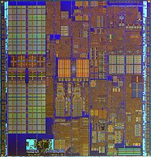
Prescott-256 Celeron D processors, initially launched June 25, 2004, featuring double the L1 cache (16 KB) and L2 cache (256 KB) as compared to the previous Willamette and Northwood desktop Celerons, by virtue of being based on the Prescott Pentium 4 core.
It also features a 533 MT/s bus and SSE3, and a 3xx model number (compared to 5xx for Pentium 4s and 7xx for Pentium Ms). The Prescott-256 Celeron D was manufactured for Socket 478 and LGA 775, with 3x0 and 3x5 designations from 310 through to 355 at clock speeds of 2.13 GHz to 3.33 GHz.
The Intel Celeron D processor works with the Intel 845 and 865 chipset families. The D suffix actually has no official designation and does not indicate that these models are dual-core. It is used simply to distinguish this line of Celeron from the previous, lower performing Northwood and Willamette series, and also from the mobile series, the Celeron M (which also uses 3xx model numbers). Unlike the Pentium D, the Celeron D is not a dual core processor.
The Celeron D was a major performance improvement over previous NetBurst-based Celerons. A test using a variety of applications, run by Derek Wilson at Anandtech.com, showed that the new Celeron D architecture alone offered up performance improvements on average of >10% over a Northwood Celeron when both CPUs were run at the same bus and clock rate. This CPU also had the addition of SSE3 instructions and the higher FSB which only contributed to this already impressive gain.
Despite its many improvements, the Prescott core of the Celeron D had at least one major drawback – heat. Unlike the fairly cool-running Northwood Celeron, the Prescott-256 had a class-rated TDP of 73 W, which prompted Intel to include a more intricate copper core/aluminum finned cooler to help handle the additional heat.
In mid-2005, Intel refreshed the Celeron D with Intel 64 and XD Bit (eXecute Disable) enabled. Model numbers increase by 1 over the previous generation (e.g., 330 became 331). This only applied to LGA 775 Celeron Ds. There are no Socket 478 CPUs with XD Bit capabilities.
In Intel's "Family/Model/Stepping" scheme, Prescott Celeron Ds and Pentium 4s are family 15, model 3 (up to stepping E0) or 4 (stepping E0 onwards), and their Intel product code is 80546 or 80547, depending on socket type.
Cedar Mill-512
Based on the Cedar Mill Pentium 4 core, this version of the Celeron D was launched May 28, 2006, and continued the 3xx naming scheme with the Celeron D 347 (3.06 GHz), 352 (3.2 GHz), 356 (3.33 GHz), 360 (3.46 GHz), and 365 (3.6 GHz). The Cedar Mill Celeron D is largely the same as the Prescott-256, except with double the L2 cache (512 KB) and based on a 65 nm manufacturing process. The Cedar Mill-512 Celeron D is LGA 775 exclusive. The main benefits of the Cedar Mill Celerons over the Prescott Celerons are the slightly increased performance due to the larger L2 cache, higher clock rates, and less heat dissipation, with several models having a TDP lowered to 65 W from Prescott's lowest offering of 73 W.
In Intel's "Family/Model/Stepping" scheme, Cedar Mill Celeron Ds and Pentium 4s are family 15, model 6, and their Intel product code is 80552.
Core-based Celerons
Main article: List of Intel Celeron microprocessors § Core based CeleronsConroe-L
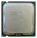
The Conroe-L Celeron is a single-core processor built on the Core microarchitecture and is thus clocked much lower than the Cedar Mill Celerons, but still outperforms them. It is based on the 65 nm Conroe-L core, and uses a 400-series model number sequence. The FSB was increased to 800 MT/s from 533 MT/s in this generation, and the TDP was decreased from 65 W to 35 W. As is traditional with Celerons, it does not have Intel VT-x instruction support or SpeedStep (although Enhanced Halt State is enabled, allowing the Celerons to lower the multiplier to 6× and decrease core voltage while idle). All Conroe-L models are single-core processors for the value segment of the market, much like the AMD K8-based Sempron. The product line was launched on June 5, 2007.
On October 21, 2007, Intel presented a new processor for its Intel Essential Series. The full name of the processor is Celeron 220 and is soldered on the D201GLY2 motherboard. With 1.2 GHz and a 512 KB L2 cache it has a TDP of 19 W and can be cooled passively. The Celeron 220 is the successor of the Celeron 215 which is based on a Yonah core and used on the D201GLY motherboard. This processor is exclusively used on the mini-ITX boards targeted to the sub-value market segment.
Allendale
Main article: Conroe (microprocessor) § AllendaleIntel launched the dual core Celeron E1xxx processor line on January 20, 2008, based on the Allendale core. The CPU has 800 MT/s FSB, 65 W TDP and uses 512 KB of the chip's 2 MB L2 cache, significantly limiting performance for uses such as gaming. New features to the Celeron family included full enhanced halt state and enhanced Intel SpeedStep technology. Clock rates range from 1.6 GHz to 2.4 GHz. It is compatible with other Allendale-based CPUs such as the Core 2 Duo E4xxx and Pentium Dual-Core E2xxx.
Wolfdale-3M
Main article: Wolfdale (microprocessor) § Wolfdale-3MThe Celeron E3000 series, starting with E3200 and E3300, was released in August 2009, featuring the Wolfdale-3M core used in Pentium Dual-Core E5000, Pentium E6000 and Core 2 Duo E7000 series. The main difference to Allendale-based Celeron processors is the support for Intel VT-x and increased performance due to the double L2 Cache of 1 MB.
Nehalem-based Celerons
Main articles: List of Intel Celeron microprocessors § Nehalem based Celerons, and List of Intel Celeron microprocessors § Nehalem based Celerons 3Clarkdale
Main article: Clarkdale (microprocessor)With the introduction of the Desktop Core i3 and Core i5 processor code named Clarkdale in January 2010, Intel also added a new Celeron line, starting with the Celeron G1101. This is the first Celeron to come with on-chip PCI Express and integrated graphics. Despite using the same Clarkdale chip as the Core i5-6xx line, it does not support Turbo Boost, HyperThreading, VT-d, SMT, Trusted Execution Technology or AES new instructions, and it comes with only 2 MB of third-level cache enabled.
Jasper Forest
Main article: Jasper Forest (microprocessor)The Celeron P1053 is an embedded processor for Socket 1366 from the Jasper Forest family. All other members of this family are known as Xeon C35xx or C55xx. The Jasper Forest chip is closely related to Lynnfield and contains four cores, 8 MB of L3 cache and a QPI interface, but most of these are disabled in the Celeron version, leaving a single core with 2 MB of L3 cache.
Sandy Bridge-based desktop Celerons
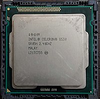
The Sandy Bridge-based Celeron processors were released in 2011. They are LGA 1155 processors (available in single- and dual-core versions) with integrated Intel HD Graphics GPU and containing up to 2 MB of L3 cache. Turbo-Boost, AVX and AES-NI have been disabled. Hyper-Threading is available on some single-core models, namely G460, G465 and G470.
Ivy Bridge-based desktop Celerons
Main article: List of Intel Celeron microprocessors § .22Ivy_Bridge.22_.2822_nm.29All Celerons of this generation belong in the G16xx series. They give some boost in performance over Sandy Bridge-based Celerons due to a 22 nm die shrink, as well as some other minor improvements.
Haswell-based desktop Celerons
Main article: Haswell (microarchitecture)Skylake-based desktop Celerons
All Celerons of this generation added AES-NI and RDRAND instruction set.
Kaby Lake-based desktop Celerons
Main article: Kaby LakeCoffee Lake-based desktop Celerons
Main article: Coffee LakeComet Lake-based desktop Celerons
Main article: Comet LakeAlder Lake-based desktop Celerons
Main article: Alder LakeMobile Celerons
P6-based mobile Celerons
Main article: List of Intel Celeron microprocessors § P6 based Celerons 2Mendocino (mobile)
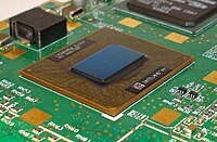
Similar to the Mendocino (Celeron-A): 250 nm, 32 KB L1 cache and 128 KB L2 cache, but uses a lower voltage (1.5–1.9 V) and two power-saving modes: Quick Start, and Deep Sleep. Packaged in the small, 615-pin BGA2 or Micro-PGA2 package.
Tualatin-256 (mobile)
These were the first Mobile Celerons based on the Tualatin core. They differed from their desktop counterparts in that the Mobile series were offered in both 100 MHz and 133 MHz FSB. Like the desktop Tualatins, these chips had 256 KB of L2 cache.
NetBurst-based mobile Celerons
Main article: List of Intel Celeron microprocessors § Netburst based Celerons 2Northwood-256
These are the Mobile Celeron range used in laptops. Also based on the Northwood core, they feature a 256 KB L2 cache. These Celeron processors were a good deal higher performing than the desktop counterparts because of their larger L2 cache sizes. They were eventually replaced by the Celeron M brand which is built around the Pentium M processor design.
Pentium M-based mobile Celerons
Main article: List of Intel Celeron microprocessors § Pentium-M based CeleronsBanias-512
This Celeron (sold under the Celeron M brand) is based on the Banias Pentium M, and differs from its parent in that it has half the L2 cache, and does not support the clock-varying SpeedStep technology. It performs reasonably well compared to the Pentium M, but battery life is noticeably shorter on a Celeron M–based notebook than it is on a comparable Pentium M notebook.
A system based on the Celeron M processor may not use the Centrino brand name, regardless of what chipset and Wi-Fi components are used.
In Intel's "Family/Model/Stepping" scheme, Banias Celeron Ms and Pentium Ms are family 6, model 9 and their Intel product code is 80535.
Shelton
The Shelton core is a Banias core without any L2 cache and SpeedStep. It is used in Intel's small form factor D845GVSH motherboard, intended for Asian and South American markets. The processor identifies itself as a "Intel Celeron 1.0B GHz", to differentiate it from the previous Coppermine-128 and Tualatin 1.0 GHz processors.
The Shelton'08 is a basic platform for a low cost notebook released by Intel at January 2008. The platform uses Intel's single-core Diamondville CPU with a clock frequency of 1.6 GHz and a 533 MT/s FSB and power consumption of 3.5 W. The platform's total power consumption is around 8 W, translating to battery usage time of between 3–4 hours. The platform consists of a 945GSE chipset, which includes built-in DirectX 9 graphics and supports single channel DDR2 memory. An 802.11g Wi-Fi module, USB/PATA port SSD (solid state drive), and a 7- or 8-inch panel will typically round out the platform.
Dothan-1024
A 90 nm Celeron M with half of the L2 cache of the 90 nm Dothan Pentium Ms (twice the L2 cache of the 130 nm Celeron Ms, though), and, like its predecessor, lacking SpeedStep. The first Celeron Ms that supports the XD bit was released in January 2005, in general any Celeron M released after that supports the XD bit. There is also a 512 KB low voltage version that was used in the early ASUS Eee PC models.
In Intel's "Family/Model/Stepping" scheme, Dothan Celeron Ms and Pentium Ms are family 6, model 13 and their Intel product code is 80536.
Yonah
Main article: Yonah (microprocessor)
The Celeron M 400-series is a 65 nm Celeron M based on the single-core Yonah chip, like the Core Solo. Like its predecessors in the Celeron M series, this Celeron M has half of the L2 cache (1 MB) of Core Solo and lacks SpeedStep. This core also brings new features to Celeron M including a higher front side bus (533 MT/s), SSE3 instructions. September 2006 and January 4, 2008, mark a discontinuation of many Celeron M branded CPUs.
Core-based mobile Celerons
Main article: List of Intel Celeron microprocessors § Core based Celerons 2Merom-L
Main article: Merom (microprocessor) § Merom-LThe Celeron M 523 (933 MHz ULV), M 520 (1.6 GHz), M 530 (1.73 GHz), 530 (1.73 GHz), 540 (1.86 GHz), 550 (2.0 GHz), 560 (2.13 GHz), 570 (2.26 GHz) are single-core 65 nm CPUs based on the Merom Core 2 architecture. They feature a 533 MT/s FSB, 1 MB of L2 cache (half that of the low end Core 2 Duo's 2 MB cache), XD-bit support, and Intel 64 technology, but lack SpeedStep and Virtualization Technology. Two different processor models are used with identical part numbers with the same part numbers, single-core Merom-L with 1 MB cache and dual-core Merom with 4 MB L2 cache that have the extra cache and core disabled. Celeron M 523, M 520 and M 530 are Socket M-based, while Celeron 530 through 570 (without the M) are for Socket P. January 4, 2008, marked the discontinuation of Merom CPUs.
Merom-2M
Main article: Merom (microprocessor) § Merom-2MThe Celeron 573 (1 GHz, ULV), 575 (2 GHz) and 585 (2.16 GHz) are based on the Merom-2M core with only one core and 1 MB L2 cache enabled. They are similar to the Merom and Merom-L based Celerons but have a faster 667 MT/s FSB.
The Celeron T1xxx processors are also based on the Merom-2M chips but have both cores enabled. The earlier T1400 (1.73 GHz) and T1500 (1.86 GHz) versions have a 533 MT/s FSB and 512 B L2 cache, while the more recent T1600 (1.66 GHz) and T1700 (1.83 GHz) versions have 667 MT/s and 1 MB L2 cache enabled but come with a lower clock frequency.
Penryn-3M
Main article: Penryn (microprocessor) § Penryn-3M
At the same time as the dual-core Merom-2M, Intel introduced the first 45 nm Celeron processor based on the Penryn-3M core with 800 MT/s FSB, 1 MB L2 cache and one core enabled. This includes the Celeron M 7xx Consumer Ultra-Low Voltage (CULV) series starting at 1.2 GHz and the later Celeron 900 (2.2 GHz).
The initial 45 nm dual-core Celeron processor was released in June 2009 and is also based on Penryn-3M. The Celeron T3000 (1.8 GHz) and T3100 (1.9 GHz) again come with 1 MB of L2 cache enabled and an 800 MT/s FSB. In September 2009, Intel also started the dual-core CULV Celeron SU2000 series, again with 1 MB L2 cache. Despite the similar name, they are very different from Pentium SU2000 (with 2 MB L2 cache and one active core) and Pentium T3000 (based on the 65 nm Merom processor).
Nehalem-based mobile Celerons
Main article: List of Intel Celeron microprocessors § Nehalem based Celerons 2Arrandale
Main article: Arrandale (microprocessor)The Arrandale-based Celeron P4xxx and U3xxx lines are low-end versions of the Pentium P6xxx and U5xxx lines, originally released as the mobile dual-core lines of Core i3/i5/i7. Like the Clarkdale-based Celeron G1xxx, they use 2 MB of L3 cache, which is the amount that the earlier "Penryn" based CPUs used in the Pentium brand as their L2 cache. Like all Arrandale processors, the Celeron P4xxx and U3xxx use an integrated graphics core.
Sandy Bridge-based mobile Celerons
Main articles: List of Intel Celeron microprocessors § Sandy Bridge based Celerons, and Sandy BridgeThe Celeron B8xx processors released in 2011 follow the Arrandale line. They are Dual-Core processors with integrated graphics and use the same chips as the Pentium B9xx and Core i3/i5/i7-2xxx mobile processors, but with Turbo-Boost, Hyper-Threading, VT-d, TXT and AES-NI disabled and the L3 cache reduced to 2MB.
Dual-processor support
As a budget processor, the Celeron does not support a dual-processor configuration using multiple CPU sockets, however it has been discovered that multiprocessing could be enabled on Slot 1 Celeron processors by connecting a pin on the CPU core to a contact on the processor card's connector. In addition, Mendocino Socket 370 processors can use multiprocessing when used on specific dual Slot 1 motherboards by using a slot adapter. The unofficial SMP support was removed in the Coppermine Celerons, and dual-socket support is now limited to higher-end Xeon server-class processors. Conroe/Allendale based Celeron processors and later support multiprocessing using multi-core chips, but are still limited to one socket.
The ABIT BP6 motherboard also allows two Mendocino Socket 370 Celeron processors to operate in a symmetric multiprocessing (SMP) configuration without any modification to the CPUs or the motherboard.
See also
References
- ^ Warren, Tom (September 16, 2022). "Intel Processor will replace Pentium and Celeron in 2023 laptops". The Verge. Retrieved December 22, 2022.
- ^ Schmid, Patrick (October 16, 2002). "The New Generation Is Here: Celeron 2.0 GHz, with 0.13 µm". Tom's Hardware Guide. Retrieved July 30, 2007.
- ^ Pabst, Thomas (April 16, 1998). "CPU Performance from Socket 7 to Slot 1". Tom's Hardware Guide. Archived from the original on February 4, 2013. Retrieved July 30, 2007.
- Cassidy, Mike (April 15, 1998). "Lexicon puts names on new technology". San Jose Mercury News.
- Slater, Michael (May 27, 1998). "Microprocessors have PCs humming". EE Times. Retrieved July 30, 2007.
- Zisman, Alex (June 1998). "Say No to Celeron". Canadian Computer Wholesaler. Retrieved July 30, 2007.
- ^ Pabst, Thomas (August 24, 1998). "Big CPU Shoot Out: Intel Launches New Celeron with Mendocino Core and Pentium II 450". Tom's Hardware Guide. Archived from the original on February 4, 2013. Retrieved July 30, 2007.
- Thomas Pabst. "How to Get All 66 MHz Slot 1 CPUs Running 100 MHz". Tom's Hardware.
- Joch, Alan (30 April 2001). "Buses: Front-side and backside". ITworld.com. Archived from the original on May 2, 2001. Retrieved July 30, 2007.
- Hachman, Mark (29 March 2000). "Intel launches Celerons with SIMD instruction-set extensions". My-ESM. Archived from the original on September 27, 2007. Retrieved July 31, 2007.
- Shimpi, Anand Lal. "Intel Celeron 600 "Coppermine128"". anandtech.com. Retrieved April 4, 2018.
- Shimpi, Anand Lal. "Intel Celeron 700". anandtech.com. Retrieved April 4, 2018.
- Lal Shimpi, Anand (January 3, 2001). "Intel Celeron 800: The first 100 MHz FSB Celeron". AnandTech. Retrieved July 30, 2007.
- Sigvartsen, Ana (October 2, 2001). "Intel's Celeron reaches 1.2 GHz". Infosatellite.com. Archived from the original on October 12, 2007. Retrieved July 31, 2007.
- Sigvartsen, Ana (7 December 2001). "Intel's Celeron gets major power boost". Infosatellite.com. Archived from the original on 12 October 2007. Retrieved 31 July 2007.
- Sigvartsen, Ana (4 January 2002). "Intel launches Celeron 1.3 GHz". Infosatellite.com. Archived from the original on 12 October 2007. Retrieved 31 July 2007.
- Sigvartsen, Ana (16 May 2002). "Intel launches Celeron with new core". Infosatellite.com. Archived from the original on 12 October 2007. Retrieved 31 July 2007.
- download.intel.com/support/processors/celeron/sb/29859604.pdf
- "Data Prefetch Logic - What is it Worth?". www.realworldtech.com. Retrieved April 4, 2018.
- Völkel, Frank; Töpelt, Bert (January 3, 2002). "Intel vs. AMD: Celeron 1300 vs. Duron 1200". Tom's Hardware Guide. Retrieved July 31, 2007.
- Schmidt, Patrick (May 15, 2002). "Good Old Newbie: Intel's 1.7 GHz Celeron for Socket 478". Tom's Hardware Guide. Retrieved July 30, 2007.
- Sigvartsen, Ana (13 June 2002). "Intel pushes Celerons to 1.8 GHz". Infosatellite.com. Archived from the original on 12 October 2007. Retrieved 30 July 2007.
- "Intel Pentium 4 Celeron processor (Willamette-128)". chiplist.com.
- Sigvartsen, Ana (17 June 2002). "Intel plans faster 0.13-micron Celeron". Infosatellite.com. Archived from the original on 12 October 2007. Retrieved 30 July 2007.
- Sigvartsen, Ana (19 September 2002). "Intel launches new Celeron, updates prices". Infosatellite.com. Archived from the original on 6 October 2007. Retrieved 30 July 2007.
- Shilov, Anton (25 June 2004). "Intel Officially Launched Celeron D Processors". X-bit labs. Archived from the original on 30 September 2007. Retrieved 31 July 2007.
- Wilson, Derek (June 24, 2004). "Intel Celeron D: New, Improved & Exceeds Expectations". AnandTech. Retrieved July 31, 2007.
- Aubrey, John (April 18, 2005). "Celeron D: the Little Processor that Could". Dev Hardware. Retrieved September 23, 2006.
- Wilson, Derek (June 24, 2004). "Intel Celeron D: New, Improved & Exceeds Expectations". AnandTech. Retrieved July 31, 2007.
- Gavrichenkov, Ilya (25 June 2004). "Intel Celeron D CPU: Budget Processors from Intel Acquire Prescott Core". X-bit labs. Archived from the original on 7 August 2007. Retrieved 31 July 2007.
- Kowaliski, Cyril (May 16, 2006). "65 nm Celeron Ds coming May 28". The Tech Report. Retrieved July 31, 2007.
- Huynh, Anh (20 September 2006). "Intel "Conroe-L" Details Unveiled". DailyTech. Archived from the original on 6 March 2012. Retrieved 23 September 2006.
- Visionary (February 13, 2007). "Intel Adds Cheapest Celeron 420 In June". VR-Zone. Archived from the original on March 3, 2007. Retrieved December 20, 2019.
- "Pentium Dual-Core E1000, Celeron 400, P35 und G33 starten offiziell". Heise News Ticker (in German). June 5, 2007. Retrieved June 13, 2007.
- "Intel Preps Dual-Core Celeron Processors". 11 October 2007. Archived from the original on 4 November 2007. Retrieved 12 November 2007.
- "ARK – Intel® Celeron® Processor G1101 (2M Cache, 2.26 GHz)". Intel® ARK (Product Specs).
- Filatova, Anna (25 June 2002). "New Mobile Celeron on Northwood-256 Core". X-bit labs. Archived from the original on 27 September 2007. Retrieved 13 March 2007.
- ^ "Intel to discontinue older Centrino CPUs in Q1 08". TG Daily. October 1, 2007. Archived from the original on November 2, 2007. Retrieved October 1, 2007.
- "Intel® Celeron® Processor". Intel® ARK (Product Specs).
- Kawada, Tomohiro. "The Dual Celeron System". Archived from the original on February 10, 2001. Retrieved November 1, 2009.
- "Intel® Celeron® Processor J Series Product Specifications". ark.intel.com. Retrieved April 2, 2019.
- "Intel Mobile Celeron (Bay Trail-M) microprocessor family". www.cpu-world.com. Retrieved April 2, 2019.
- "Intel Mobile Celeron (Braswell) microprocessor family". www.cpu-world.com. Retrieved April 2, 2019.
- "Intel Mobile Celeron (Gemini Lake) microprocessor family". www.cpu-world.com. Retrieved April 2, 2019.
- "Intel Mobile Celeron (Apollo Lake) microprocessor family". www.cpu-world.com. Retrieved April 2, 2019.
- "Braswell - Cores - Intel - WikiChip". en.wikichip.org. Retrieved April 2, 2019.
- "Apollo Lake: Overview". Intel. Retrieved April 2, 2019.
External links
- Intel Celeron M Processor – Product overview
- Intel Celeron M Banias, Dothan, and Yonah specifications
- Intel Pentium II and Pentium III based Celerons at cpu-collection.de
- Intel CPU Transition Roadmap 2008–2013
- Intel Desktop CPU Roadmap 2004–2011
- Intel Mobile CPU Roadmap 2004–2011
| Intel processors | |||||||||||||||
|---|---|---|---|---|---|---|---|---|---|---|---|---|---|---|---|
| Lists | |||||||||||||||
| Microarchitectures |
| ||||||||||||||
| Current products |
| ||||||||||||||
| Discontinued |
| ||||||||||||||
| Related | |||||||||||||||
Categories: